

133
Strain-Engineered MOSFETs
larger strain effects. FinFET with condensed SiGe S/D also shows a larger
peak transconductance than the control device, as observed in Figure 5.12(a),
indicating a higher hole mobility, which can be attributed to the enhanced
strain effect. As shown in Figure 5.12(b), the two devices have comparable
source/drain series resistances.
5.7 Stress-Engineered FinFETs
The technique of inducing stress by using a tensile (for n-MOSFET) or
compressive (for p-MOSFET) SiN x capping layer is attractive because of its
relatively simple process and its extendibility from bulk Si to silicon-oninsulator (SOI) MOSFETs. In this section, the impact of tensile and compressive capping layers on electron and hole mobilities is investigated for Si fins
with {100} sidewalls and <100> current flow direction, and Si fins with {110}
sidewalls and <110> current flow direction, which are optimal for maximum
electron and hole mobilities, respectively [7, 8]. The effects of various structural parameters (gate electrode thickness, gate length, and fin aspect ratio)
need to be studied to provide insight for strain engineering in nonplanar
FinFET structures.
–1.5
10
–11
10
–10
10 –9
10 –8
Drain Current I
D (A/µm)
Drain Current I
D (µA/µm)
10
–7
10
–6
10
–5
10
–4
10
–3
350
V D = –0.05, –1.2 V
V G = V th = –1.2 V
Step = –0.4 V
L G = 26 nm
Control
Condensed
SiGeS/D
Control
Condensed SiGeS/D
W = 0.1 µm
300
250
200
150
100
50
0
–1.0 –0.5 0.0
Gate Voltage V G (V)
(a)
0.5 1.0
–2.0 –1.5 –1.0
Drain Voltage V D (V)
(b)
–0.5
0.0
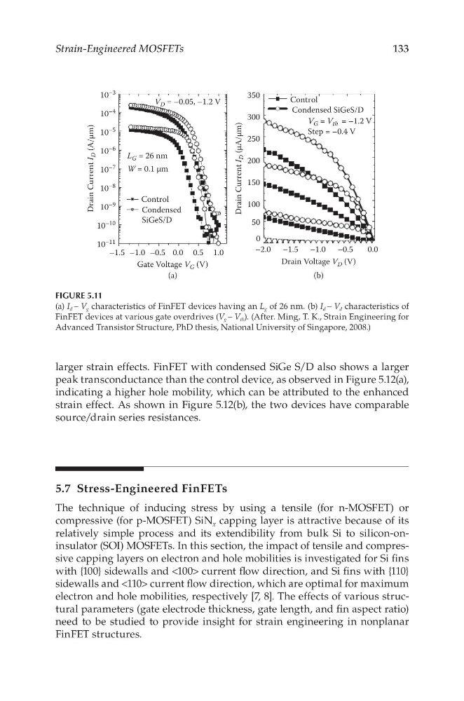
FIGURE 5.11
(a) I d – V g characteristics of FinFET devices having an L g of 26 nm. (b) I d – V d characteristics of
FinFET devices at various gate overdrives (V g – V th ). (After. Ming, T. K., Strain Engineering for
Advanced Transistor Structure, PhD thesis, National University of Singapore, 2008.)
Strain-Engineered MOSFETs
larger strain effects. FinFET with condensed SiGe S/D also shows a larger
peak transconductance than the control device, as observed in Figure 5.12(a),
indicating a higher hole mobility, which can be attributed to the enhanced
strain effect. As shown in Figure 5.12(b), the two devices have comparable
source/drain series resistances.
5.7 Stress-Engineered FinFETs
The technique of inducing stress by using a tensile (for n-MOSFET) or
compressive (for p-MOSFET) SiN x capping layer is attractive because of its
relatively simple process and its extendibility from bulk Si to silicon-oninsulator (SOI) MOSFETs. In this section, the impact of tensile and compressive capping layers on electron and hole mobilities is investigated for Si fins
with {100} sidewalls and <100> current flow direction, and Si fins with {110}
sidewalls and <110> current flow direction, which are optimal for maximum
electron and hole mobilities, respectively [7, 8]. The effects of various structural parameters (gate electrode thickness, gate length, and fin aspect ratio)
need to be studied to provide insight for strain engineering in nonplanar
FinFET structures.
–1.5
10
–11
10
–10
10 –9
10 –8
Drain Current I
D (A/µm)
Drain Current I
D (µA/µm)
10
–7
10
–6
10
–5
10
–4
10
–3
350
V D = –0.05, –1.2 V
V G = V th = –1.2 V
Step = –0.4 V
L G = 26 nm
Control
Condensed
SiGeS/D
Control
Condensed SiGeS/D
W = 0.1 µm
300
250
200
150
100
50
0
–1.0 –0.5 0.0
Gate Voltage V G (V)
(a)
0.5 1.0
–2.0 –1.5 –1.0
Drain Voltage V D (V)
(b)
–0.5
0.0
FIGURE 5.11
(a) I d – V g characteristics of FinFET devices having an L g of 26 nm. (b) I d – V d characteristics of
FinFET devices at various gate overdrives (V g – V th ). (After. Ming, T. K., Strain Engineering for
Advanced Transistor Structure, PhD thesis, National University of Singapore, 2008.)