

132
Strain-Engineered MOSFETs
than the control FinFET. The subthreshold swing of the devices is comparable, as shown in Figure 5.9(b). Furthermore, they also demonstrate similar
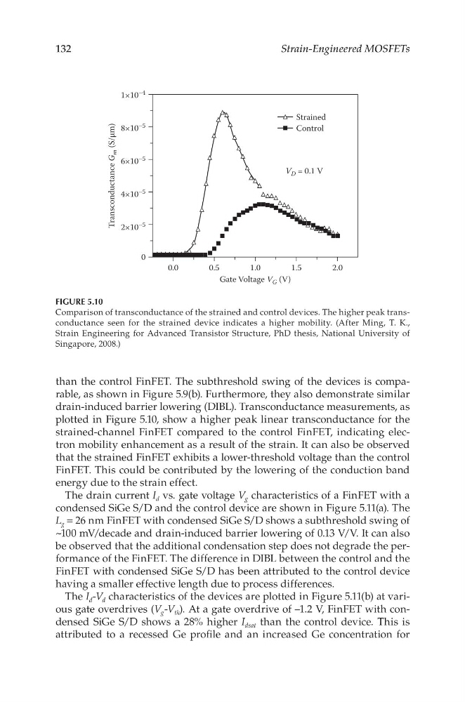
drain-induced barrier lowering (DIBL). Transconductance measurements, as
plotted in Figure 5.10, show a higher peak linear transconductance for the
strained-channel FinFET compared to the control FinFET, indicating electron mobility enhancement as a result of the strain. It can also be observed
that the strained FinFET exhibits a lower-threshold voltage than the control
FinFET. This could be contributed by the lowering of the conduction band
energy due to the strain effect.
The drain current I d vs. gate voltage V g characteristics of a FinFET with a
condensed SiGe S/D and the control device are shown in Figure 5.11(a). The
L g = 26 nm FinFET with condensed SiGe S/D shows a subthreshold swing of
~100 mV/decade and drain-induced barrier lowering of 0.13 V/V. It can also
be observed that the additional condensation step does not degrade the performance of the FinFET. The difference in DIBL between the control and the
FinFET with condensed SiGe S/D has been attributed to the control device
having a smaller effective length due to process differences.
The I d -V d characteristics of the devices are plotted in Figure 5.11(b) at various gate overdrives (V g -V th ). At a gate overdrive of –1.2 V, FinFET with condensed SiGe S/D shows a 28% higher I dsat than the control device. This is
attributed to a recessed Ge profile and an increased Ge concentration for
1×10
–4
8×10
–5
6×10 –5
4×10
–5
Transconductance G
m (S/µm)
2×10
–5
0
0.0
0.5
Strained
Control
Gate Voltage V G (V)
V D = 0.1 V
1.0
1.5
2.0
FIGURE 5.10
Comparison of transconductance of the strained and control devices. The higher peak transconductance seen for the strained device indicates a higher mobility. (After Ming, T. K.,
Strain Engineering for Advanced Transistor Structure, PhD thesis, National University of
Singapore, 2008.)
Strain-Engineered MOSFETs
than the control FinFET. The subthreshold swing of the devices is comparable, as shown in Figure 5.9(b). Furthermore, they also demonstrate similar
drain-induced barrier lowering (DIBL). Transconductance measurements, as
plotted in Figure 5.10, show a higher peak linear transconductance for the
strained-channel FinFET compared to the control FinFET, indicating electron mobility enhancement as a result of the strain. It can also be observed
that the strained FinFET exhibits a lower-threshold voltage than the control
FinFET. This could be contributed by the lowering of the conduction band
energy due to the strain effect.
The drain current I d vs. gate voltage V g characteristics of a FinFET with a
condensed SiGe S/D and the control device are shown in Figure 5.11(a). The
L g = 26 nm FinFET with condensed SiGe S/D shows a subthreshold swing of
~100 mV/decade and drain-induced barrier lowering of 0.13 V/V. It can also
be observed that the additional condensation step does not degrade the performance of the FinFET. The difference in DIBL between the control and the
FinFET with condensed SiGe S/D has been attributed to the control device
having a smaller effective length due to process differences.
The I d -V d characteristics of the devices are plotted in Figure 5.11(b) at various gate overdrives (V g -V th ). At a gate overdrive of –1.2 V, FinFET with condensed SiGe S/D shows a 28% higher I dsat than the control device. This is
attributed to a recessed Ge profile and an increased Ge concentration for
1×10
–4
8×10
–5
6×10 –5
4×10
–5
Transconductance G
m (S/µm)
2×10
–5
0
0.0
0.5
Strained
Control
Gate Voltage V G (V)
V D = 0.1 V
1.0
1.5
2.0
FIGURE 5.10
Comparison of transconductance of the strained and control devices. The higher peak transconductance seen for the strained device indicates a higher mobility. (After Ming, T. K.,
Strain Engineering for Advanced Transistor Structure, PhD thesis, National University of
Singapore, 2008.)