

131
Strain-Engineered MOSFETs
800
600
400
Drain Current I
D (µA/µm)
200
0
0.0
0.5
1.0
Drain Voltage V D (V)
1.5
2.0
2.5
Control
Strained
L G = 75 nm
V GS – V th = 2.0 V
V GS – V th = 1.5 V
V GS – V th = 1.0 V
V GS – V th = 0.5 V
V GS – V th = 0 V
H n = 45 nm
10
–3
10
–4
10
–5
10
–6
10
–7
10
–8
Drain Current I
D (µA/µm)
–0.5
0.0
1.0
0.5
Drain Voltage V G (V)
(a)
(b)
1.5
2.0
2.5
Control
Strained
V D = 1.8 V
V D = 0.1 V
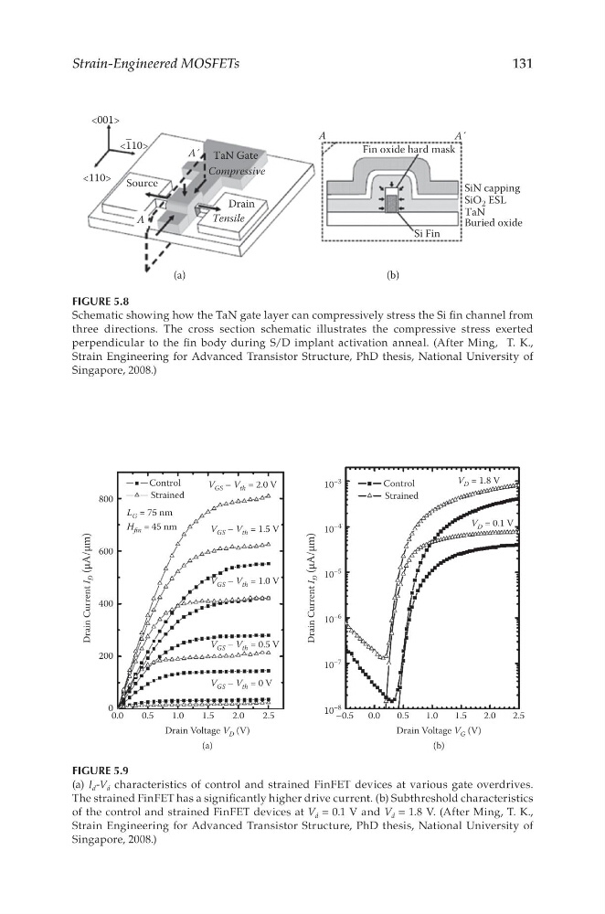
FIGURE 5.9
(a) I d -V d characteristics of control and strained FinFET devices at various gate overdrives.
The strained FinFET has a significantly higher drive current. (b) Subthreshold characteristics
of the control and strained FinFET devices at V d = 0.1 V and V d = 1.8 V. (After Ming, T. K.,
Strain Engineering for Advanced Transistor Structure, PhD thesis, National University of
Singapore, 2008.)
<001>
<110> Source
A
A
A´
A´
Si Fin
SiN capping
SiO 2 ESL
TaN
Buried oxide
Fin oxide hard mask
TaN Gate
Compressive
Tensile
Drain
(a)
(b)
–
<110>
FIGURE 5.8
Schematic showing how the TaN gate layer can compressively stress the Si fin channel from
three directions. The cross section schematic illustrates the compressive stress exerted
perpendicular to the fin body during S/D implant activation anneal. (After Ming, T. K.,
Strain Engineering for Advanced Transistor Structure, PhD thesis, National University of
Singapore, 2008.)
Strain-Engineered MOSFETs
800
600
400
Drain Current I
D (µA/µm)
200
0
0.0
0.5
1.0
Drain Voltage V D (V)
1.5
2.0
2.5
Control
Strained
L G = 75 nm
V GS – V th = 2.0 V
V GS – V th = 1.5 V
V GS – V th = 1.0 V
V GS – V th = 0.5 V
V GS – V th = 0 V
H n = 45 nm
10
–3
10
–4
10
–5
10
–6
10
–7
10
–8
Drain Current I
D (µA/µm)
–0.5
0.0
1.0
0.5
Drain Voltage V G (V)
(a)
(b)
1.5
2.0
2.5
Control
Strained
V D = 1.8 V
V D = 0.1 V
FIGURE 5.9
(a) I d -V d characteristics of control and strained FinFET devices at various gate overdrives.
The strained FinFET has a significantly higher drive current. (b) Subthreshold characteristics
of the control and strained FinFET devices at V d = 0.1 V and V d = 1.8 V. (After Ming, T. K.,
Strain Engineering for Advanced Transistor Structure, PhD thesis, National University of
Singapore, 2008.)
<001>
<110> Source
A
A
A´
A´
Si Fin
SiN capping
SiO 2 ESL
TaN
Buried oxide
Fin oxide hard mask
TaN Gate
Compressive
Tensile
Drain
(a)
(b)
–
<110>
FIGURE 5.8
Schematic showing how the TaN gate layer can compressively stress the Si fin channel from
three directions. The cross section schematic illustrates the compressive stress exerted
perpendicular to the fin body during S/D implant activation anneal. (After Ming, T. K.,
Strain Engineering for Advanced Transistor Structure, PhD thesis, National University of
Singapore, 2008.)