

129
Strain-Engineered MOSFETs
The contact resistance between the via and silicided S/D region is dominated
by the contact area and work function difference between the two metallic
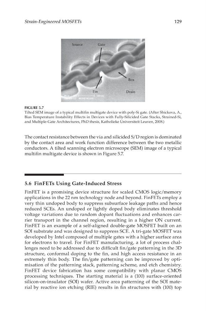
conductors. A tilted scanning electron microscope (SEM) image of a typical
multifin multigate device is shown in Figure 5.7.
5.6 FinFETs Using Gate-Induced Stress
FinFET is a promising device structure for scaled CMOS logic/memory
applications in the 22 nm technology node and beyond. FinFETs employ a
very thin undoped body to suppress subsurface leakage paths and hence
reduced SCEs. An undoped or lightly doped body eliminates threshold
voltage variations due to random dopant fluctuations and enhances carrier transport in the channel region, resulting in a higher ON current.
FinFET is an example of a self-aligned double-gate MOSFET built on an
SOI substrate and was designed to suppress SCE. A tri-gate MOSFET was
developed by Intel composed of multiple gates with a higher surface area
for electrons to travel. For FinFET manufacturing, a lot of process challenges need to be addressed due to difficult fin/gate patterning in the 3D
structure, conformal doping to the fin, and high access resistance in an
extremely thin body. The fin/gate patterning can be improved by optimisation of the patterning stack, patterning scheme, and etch chemistry.
FinFET device fabrication has some compatibility with planar CMOS
processing techniques. The starting material is a (100) surface-oriented
silicon-on-insulator (SOI) wafer. Active area patterning of the SOI material by reactive ion etching (RIE) results in fin structures with (100) top
Source
Gate
Box
Drain
Fin
FIGURE 5.7
Tilted SEM image of a typical multifin multigate device with poly-Si gate. (After Shickova, A.,
Bias Temperature Instability Effects in Devices with Fully-Silicided Gate Stacks, Strained-Si,
and Multiple-Gate Architectures, PhD thesis, Katholieke Universiteit Leuven, 2008.)
Strain-Engineered MOSFETs
The contact resistance between the via and silicided S/D region is dominated
by the contact area and work function difference between the two metallic
conductors. A tilted scanning electron microscope (SEM) image of a typical
multifin multigate device is shown in Figure 5.7.
5.6 FinFETs Using Gate-Induced Stress
FinFET is a promising device structure for scaled CMOS logic/memory
applications in the 22 nm technology node and beyond. FinFETs employ a
very thin undoped body to suppress subsurface leakage paths and hence
reduced SCEs. An undoped or lightly doped body eliminates threshold
voltage variations due to random dopant fluctuations and enhances carrier transport in the channel region, resulting in a higher ON current.
FinFET is an example of a self-aligned double-gate MOSFET built on an
SOI substrate and was designed to suppress SCE. A tri-gate MOSFET was
developed by Intel composed of multiple gates with a higher surface area
for electrons to travel. For FinFET manufacturing, a lot of process challenges need to be addressed due to difficult fin/gate patterning in the 3D
structure, conformal doping to the fin, and high access resistance in an
extremely thin body. The fin/gate patterning can be improved by optimisation of the patterning stack, patterning scheme, and etch chemistry.
FinFET device fabrication has some compatibility with planar CMOS
processing techniques. The starting material is a (100) surface-oriented
silicon-on-insulator (SOI) wafer. Active area patterning of the SOI material by reactive ion etching (RIE) results in fin structures with (100) top
Source
Gate
Box
Drain
Fin
FIGURE 5.7
Tilted SEM image of a typical multifin multigate device with poly-Si gate. (After Shickova, A.,
Bias Temperature Instability Effects in Devices with Fully-Silicided Gate Stacks, Strained-Si,
and Multiple-Gate Architectures, PhD thesis, Katholieke Universiteit Leuven, 2008.)