

128
Strain-Engineered MOSFETs
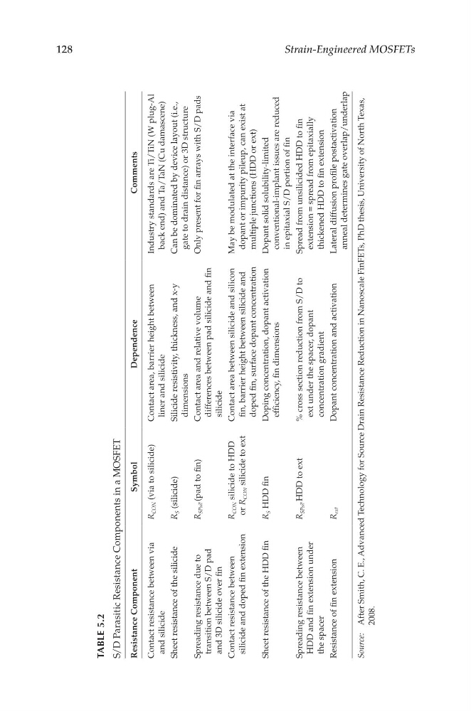
TABLE 5.2
S/D Parasitic Resistance Components in a MOSFET
Resistance Component
Symbol
Dependence
Comments
Contact resistance between via
and silicide
R
CON (via to silicide)
Contact area, barrier height between
liner and silicide
Industry standards are Ti/TiN (W plug-Al
back end) and Ta/TaN (Cu damascene)
Sheet resistance of the silicide
R
S (silicide)
Silicide resistivity, thickness, and x-y
dimensions
Can be dominated by device layout (i.e.,
gate to drain distance) or 3D structure
Spreading resistance due to
transition between S/D pad
and 3D silicide over fin
R
SPsil (pad to fin)
Contact area and relative volume
differences between pad silicide and fin
silicide
Only present for fin arrays with S/D pads
Contact resistance between
silicide and doped fin extension
R
CON silicide to HDD
or R
CON silicide to ext
Contact area between silicide and silicon
fin, barrier height between silicide and
doped fin, surface dopant concentration
May be modulated at the interface via
dopant or impurity pileup, can exist at
multiple junctions (HDD or ext)
Sheet resistance of the HDD fin
R
S HDD fin
Doping concentration, dopant activation
efficiency, fin dimensions
Dopant solid solubility-limited
conventional-implant issues are reduced
in epitaxial S/D portion of fin
Spreading resistance between
HDD and fin extension under
the spacer
R
SPsil HDD to ext
% cross section reduction from S/D to
ext under the spacer, dopant
concentration gradient
Spread from unsilicided HDD to fin
extension
= spread from epitaxially
thickened HDD to fin extension
Resistance of fin extension
R
ext
Dopant concentration and activation
Lateral diffusion profile postactivation
anneal determines gate overlap/underlap
Source:
After Smith, C. E., Advanced Technology for Source Drain Resistance Reduction in Nanoscale FinFETs, PhD thesis, University of North Texas,
2008.
Strain-Engineered MOSFETs
TABLE 5.2
S/D Parasitic Resistance Components in a MOSFET
Resistance Component
Symbol
Dependence
Comments
Contact resistance between via
and silicide
R
CON (via to silicide)
Contact area, barrier height between
liner and silicide
Industry standards are Ti/TiN (W plug-Al
back end) and Ta/TaN (Cu damascene)
Sheet resistance of the silicide
R
S (silicide)
Silicide resistivity, thickness, and x-y
dimensions
Can be dominated by device layout (i.e.,
gate to drain distance) or 3D structure
Spreading resistance due to
transition between S/D pad
and 3D silicide over fin
R
SPsil (pad to fin)
Contact area and relative volume
differences between pad silicide and fin
silicide
Only present for fin arrays with S/D pads
Contact resistance between
silicide and doped fin extension
R
CON silicide to HDD
or R
CON silicide to ext
Contact area between silicide and silicon
fin, barrier height between silicide and
doped fin, surface dopant concentration
May be modulated at the interface via
dopant or impurity pileup, can exist at
multiple junctions (HDD or ext)
Sheet resistance of the HDD fin
R
S HDD fin
Doping concentration, dopant activation
efficiency, fin dimensions
Dopant solid solubility-limited
conventional-implant issues are reduced
in epitaxial S/D portion of fin
Spreading resistance between
HDD and fin extension under
the spacer
R
SPsil HDD to ext
% cross section reduction from S/D to
ext under the spacer, dopant
concentration gradient
Spread from unsilicided HDD to fin
extension
= spread from epitaxially
thickened HDD to fin extension
Resistance of fin extension
R
ext
Dopant concentration and activation
Lateral diffusion profile postactivation
anneal determines gate overlap/underlap
Source:
After Smith, C. E., Advanced Technology for Source Drain Resistance Reduction in Nanoscale FinFETs, PhD thesis, University of North Texas,
2008.