

127
Strain-Engineered MOSFETs
5.5 Tri-Gate FinFET
Tri-gate transistors employ a single gate stacked on top of two vertical gates,
allowing for essentially three times the surface area for carriers to travel. In the
technical literature, the term tri-gate is sometimes used generically to denote
any multigate FET with three effective gates or channels. The tri-gate devices
having more geometrical dimensions than the planar devices are exposed to a
risk from electric field concentration around the fin corners. This corner effect
is alleviated by appropriate corner rounding processing. For strained tri-gate
FinFETs, contributions from the top gate and the sidewalls should be studied
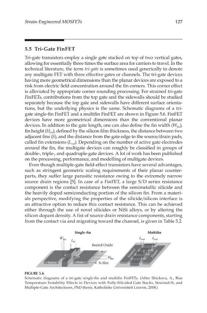
separately because the top gate and sidewalls have different surface orientations, but the underlying physics is the same. Schematic diagrams of a trigate single-fin FinFET and a multifin FinFET are shown in Figure 5.6. FinFET
devices have more geometrical dimensions than the conventional planar
devices. In addition to the gate length, one can also define the fin width (W fin ),
fin height (H fin ), defined by the silicon film thickness, the distance between two
adjacent fins (S), and the distance from the gate edge to the source/drain pads,
called fin extensions (L ext ). Depending on the number of active gate electrodes
around the fin, the multigate devices can roughly be classified in groups of
double-, triple-, and quadruple-gate devices. A lot of work has been published
on the processing, performance, and modelling of multigate devices.
Even though multiple-gate field-effect transistors have several advantages,
such as stringent geometric scaling requirements of their planar counterparts, they suffer large parasitic resistance owing to the extremely narrow
source drain regions [5]. In case of a FinFET, a large S/D series resistance
component is the contact resistance between the semimetallic silicide and
the heavily doped semiconducting portion of the silicon fin. From a materials perspective, modifying the properties of the silicide/silicon interface is
an attractive option to reduce this contact resistance. This can be achieved
either through the use of novel silicides or NiSi alloys, or by altering the
silicon dopant density. A list of source drain resistance components, starting
from the contact via and migrating toward the channel, is given in Table 5.2.
Single-fin
Buried Oxide
Drain
Source
Multifin
W fin
fin
H fin
L G
Si film
S
D r a i n
S o u r c e
L ext
L ext
FIGURE 5.6
Schematic diagrams of a tri-gate single-fin and multifin FinFETs. (After Shickova, A., Bias
Temperature Instability Effects in Devices with Fully-Silicided Gate Stacks, Strained-Si, and
Multiple-Gate Architectures, PhD thesis, Katholieke Universiteit Leuven, 2008.)
Strain-Engineered MOSFETs
5.5 Tri-Gate FinFET
Tri-gate transistors employ a single gate stacked on top of two vertical gates,
allowing for essentially three times the surface area for carriers to travel. In the
technical literature, the term tri-gate is sometimes used generically to denote
any multigate FET with three effective gates or channels. The tri-gate devices
having more geometrical dimensions than the planar devices are exposed to a
risk from electric field concentration around the fin corners. This corner effect
is alleviated by appropriate corner rounding processing. For strained tri-gate
FinFETs, contributions from the top gate and the sidewalls should be studied
separately because the top gate and sidewalls have different surface orientations, but the underlying physics is the same. Schematic diagrams of a trigate single-fin FinFET and a multifin FinFET are shown in Figure 5.6. FinFET
devices have more geometrical dimensions than the conventional planar
devices. In addition to the gate length, one can also define the fin width (W fin ),
fin height (H fin ), defined by the silicon film thickness, the distance between two
adjacent fins (S), and the distance from the gate edge to the source/drain pads,
called fin extensions (L ext ). Depending on the number of active gate electrodes
around the fin, the multigate devices can roughly be classified in groups of
double-, triple-, and quadruple-gate devices. A lot of work has been published
on the processing, performance, and modelling of multigate devices.
Even though multiple-gate field-effect transistors have several advantages,
such as stringent geometric scaling requirements of their planar counterparts, they suffer large parasitic resistance owing to the extremely narrow
source drain regions [5]. In case of a FinFET, a large S/D series resistance
component is the contact resistance between the semimetallic silicide and
the heavily doped semiconducting portion of the silicon fin. From a materials perspective, modifying the properties of the silicide/silicon interface is
an attractive option to reduce this contact resistance. This can be achieved
either through the use of novel silicides or NiSi alloys, or by altering the
silicon dopant density. A list of source drain resistance components, starting
from the contact via and migrating toward the channel, is given in Table 5.2.
Single-fin
Buried Oxide
Drain
Source
Multifin
W fin
fin
H fin
L G
Si film
S
D r a i n
S o u r c e
L ext
L ext
FIGURE 5.6
Schematic diagrams of a tri-gate single-fin and multifin FinFETs. (After Shickova, A., Bias
Temperature Instability Effects in Devices with Fully-Silicided Gate Stacks, Strained-Si, and
Multiple-Gate Architectures, PhD thesis, Katholieke Universiteit Leuven, 2008.)