

126
Strain-Engineered MOSFETs
control of the electric field. The Ω-FinFETs have unique features, such as high
heat dissipation to the Si substrate, no floating body effect, and low defect
density, while having the key advantages of the silicon-on-insulator (SOI)based CMOS technology. The Ω-FinFET has a top gate like the conventional
UTB-SOI, sidewall gates like FinFETs, and special gate extensions under the
silicon body. The Ω-FinFET is basically a field-effect transistor with a gate
that almost covers the body. However, the manufacturability of these types
of device structures is still an issue. Many methods have been proposed to
fabricate these devices, but most of them suffer from technical challenges,
mainly due to the process complexity. Aggressively scaled FinFET structures
suffer significantly from degraded device performance due to large source/
drain series resistance, and to mitigate, several methods such as maximising contact area, silicide engineering, and epitaxially raised S/D have been
explored. Strained Si technology is beneficial for enhancing carrier mobilities to boost I on . Both electron and hole mobilities can be improved by applying stress to induce appropriate strain in the channel, e.g., tensile strain for
n-MOSFETs and compressive strain for p-MOSFETs. The effect of strain on
mobility can be understood by considering the stress-induced changes in the
electronic band structures of Si.
The novel device designs require 3D process and device simulations.
FinFET is a nonplanar device and is inherently 3D in nature. Therefore, for
FinFETs, any meaningful process or device simulation must be performed
in three dimensions. Synopsys tools such as SProcess and SDevice address
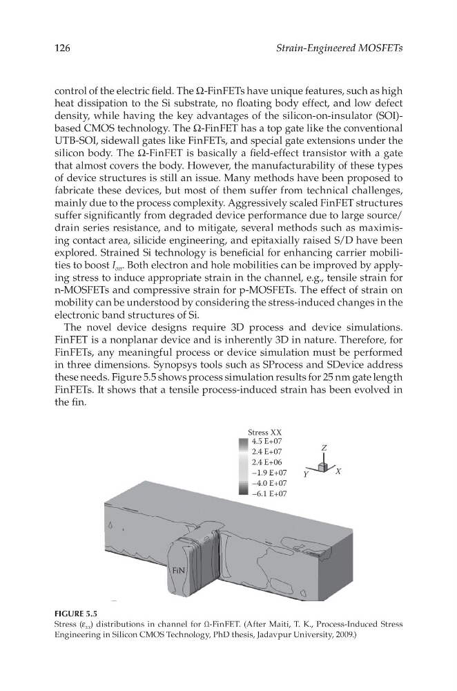
these needs. Figure 5.5 shows process simulation results for 25 nm gate length
FinFETs. It shows that a tensile process-induced strain has been evolved in
the fin.
4.5 E+07
Stress XX
Y
Z
X
2.4 E+07
2.4 E+06
–1.9 E+07
FiN
–4.0 E+07
–6.1 E+07
FIGURE 5.5
Stress (ε xx ) distributions in channel for Ω-FinFET. (After Maiti, T. K., Process-Induced Stress
Engineering in Silicon CMOS Technology, PhD thesis, Jadavpur University, 2009.)
Strain-Engineered MOSFETs
control of the electric field. The Ω-FinFETs have unique features, such as high
heat dissipation to the Si substrate, no floating body effect, and low defect
density, while having the key advantages of the silicon-on-insulator (SOI)based CMOS technology. The Ω-FinFET has a top gate like the conventional
UTB-SOI, sidewall gates like FinFETs, and special gate extensions under the
silicon body. The Ω-FinFET is basically a field-effect transistor with a gate
that almost covers the body. However, the manufacturability of these types
of device structures is still an issue. Many methods have been proposed to
fabricate these devices, but most of them suffer from technical challenges,
mainly due to the process complexity. Aggressively scaled FinFET structures
suffer significantly from degraded device performance due to large source/
drain series resistance, and to mitigate, several methods such as maximising contact area, silicide engineering, and epitaxially raised S/D have been
explored. Strained Si technology is beneficial for enhancing carrier mobilities to boost I on . Both electron and hole mobilities can be improved by applying stress to induce appropriate strain in the channel, e.g., tensile strain for
n-MOSFETs and compressive strain for p-MOSFETs. The effect of strain on
mobility can be understood by considering the stress-induced changes in the
electronic band structures of Si.
The novel device designs require 3D process and device simulations.
FinFET is a nonplanar device and is inherently 3D in nature. Therefore, for
FinFETs, any meaningful process or device simulation must be performed
in three dimensions. Synopsys tools such as SProcess and SDevice address
these needs. Figure 5.5 shows process simulation results for 25 nm gate length
FinFETs. It shows that a tensile process-induced strain has been evolved in
the fin.
4.5 E+07
Stress XX
Y
Z
X
2.4 E+07
2.4 E+06
–1.9 E+07
FiN
–4.0 E+07
–6.1 E+07
FIGURE 5.5
Stress (ε xx ) distributions in channel for Ω-FinFET. (After Maiti, T. K., Process-Induced Stress
Engineering in Silicon CMOS Technology, PhD thesis, Jadavpur University, 2009.)