

125
Strain-Engineered MOSFETs
with the bulk Si MOSFET. Enhancement of multigate performance via
process-induced strain has been investigated recently by several groups. The
effects of strain on the performance of n-channel and p-channel multigate
with {110}/<110> and {100}/<100> surface orientation/current direction have
also been addressed.
5.4 Ω-FinFET
Ω-FinFET is known to be the most manufacturable structure due to selfaligned gate electrodes compatible with the conventional planar bulk CMOS
process. The Ω-FinFET design, named after the similarity between the
Greek letter omega and the shape in which the gate wraps around the fin, is
another variation of the tri-gate structure. The fin undercut allows the gate
electrodes to extend partially below the fin, and in this way to offer better
Gate
Gate
Gate
Drain
Drain
Si (100)
Multi-gate structure for
better control of SCE
(a)
(b)
(c)
Si (01–1)
Si (100)
SiO 2
SiO 2
<011>
SiO 2
Source
Source
Source
Si n
Si n
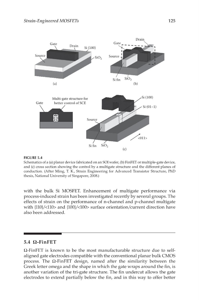
FIGURE 5.4
Schematics of a (a) planar device fabricated on an SOI wafer, (b) FinFET or multiple-gate device,
and (c) cross section showing the control by a multigate structure and the different planes of
conduction. (After Ming, T. K., Strain Engineering for Advanced Transistor Structure, PhD
thesis, National University of Singapore, 2008.)
Strain-Engineered MOSFETs
with the bulk Si MOSFET. Enhancement of multigate performance via
process-induced strain has been investigated recently by several groups. The
effects of strain on the performance of n-channel and p-channel multigate
with {110}/<110> and {100}/<100> surface orientation/current direction have
also been addressed.
5.4 Ω-FinFET
Ω-FinFET is known to be the most manufacturable structure due to selfaligned gate electrodes compatible with the conventional planar bulk CMOS
process. The Ω-FinFET design, named after the similarity between the
Greek letter omega and the shape in which the gate wraps around the fin, is
another variation of the tri-gate structure. The fin undercut allows the gate
electrodes to extend partially below the fin, and in this way to offer better
Gate
Gate
Gate
Drain
Drain
Si (100)
Multi-gate structure for
better control of SCE
(a)
(b)
(c)
Si (01–1)
Si (100)
SiO 2
SiO 2
<011>
SiO 2
Source
Source
Source
Si n
Si n
FIGURE 5.4
Schematics of a (a) planar device fabricated on an SOI wafer, (b) FinFET or multiple-gate device,
and (c) cross section showing the control by a multigate structure and the different planes of
conduction. (After Ming, T. K., Strain Engineering for Advanced Transistor Structure, PhD
thesis, National University of Singapore, 2008.)