

123
Strain-Engineered MOSFETs
5.3 Double-Gate MOSFET
The double-gate (DG) MOSFET is a promising structure for scaling CMOS
into the sub-15 nm gate length regime because of its excellent suppression
of short-channel effects (SCEs) for a given equivalent gate oxide thickness.
Planar double-gate transistors take advantage of the conventional planar
manufacturing processes to create double-gate devices, avoiding more difficult lithography requirements associated with nonplanar, vertical transistor structures. In planar double-gate transistors the channel is positioned
between two independently fabricated gate oxide stacks. The addition of
the second gate electrode helps to control the potential lines, originating
Planar
double-gate
Vertical
double-gate
HM
Tri-Gate
Ω-Gate
Π-Gate
G AA
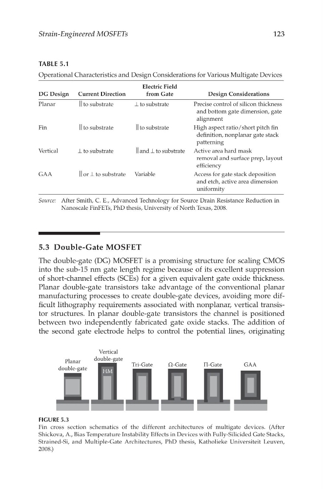
FIGURE 5.3
Fin cross section schematics of the different architectures of multigate devices. (After
Shickova, A., Bias Temperature Instability Effects in Devices with Fully-Silicided Gate Stacks,
Strained-Si, and Multiple-Gate Architectures, PhD thesis, Katholieke Universiteit Leuven,
2008.)
TABLE 5.1
Operational Characteristics and Design Considerations for Various Multigate Devices
DG Design
Current Direction
Electric Field
from Gate
Design Considerations
Planar
⎥⎥ to substrate
⊥ to substrate
Precise control of silicon thickness
and bottom gate dimension, gate
alignment
Fin
⎥⎥ to substrate
⎥⎥ to substrate
High aspect ratio/short pitch fin
definition, nonplanar gate stack
patterning
Vertical
⊥ to substrate
⎥⎥ and ⊥ to substrate
Active area hard mask
removal and surface prep, layout
efficiency
GAA
⎥⎥ or ⊥ to substrate
Variable
Access for gate stack deposition
and etch, active area dimension
uniformity
Source: After Smith, C. E., Advanced Technology for Source Drain Resistance Reduction in
Nanoscale FinFETs, PhD thesis, University of North Texas, 2008.
Strain-Engineered MOSFETs
5.3 Double-Gate MOSFET
The double-gate (DG) MOSFET is a promising structure for scaling CMOS
into the sub-15 nm gate length regime because of its excellent suppression
of short-channel effects (SCEs) for a given equivalent gate oxide thickness.
Planar double-gate transistors take advantage of the conventional planar
manufacturing processes to create double-gate devices, avoiding more difficult lithography requirements associated with nonplanar, vertical transistor structures. In planar double-gate transistors the channel is positioned
between two independently fabricated gate oxide stacks. The addition of
the second gate electrode helps to control the potential lines, originating
Planar
double-gate
Vertical
double-gate
HM
Tri-Gate
Ω-Gate
Π-Gate
G AA
FIGURE 5.3
Fin cross section schematics of the different architectures of multigate devices. (After
Shickova, A., Bias Temperature Instability Effects in Devices with Fully-Silicided Gate Stacks,
Strained-Si, and Multiple-Gate Architectures, PhD thesis, Katholieke Universiteit Leuven,
2008.)
TABLE 5.1
Operational Characteristics and Design Considerations for Various Multigate Devices
DG Design
Current Direction
Electric Field
from Gate
Design Considerations
Planar
⎥⎥ to substrate
⊥ to substrate
Precise control of silicon thickness
and bottom gate dimension, gate
alignment
Fin
⎥⎥ to substrate
⎥⎥ to substrate
High aspect ratio/short pitch fin
definition, nonplanar gate stack
patterning
Vertical
⊥ to substrate
⎥⎥ and ⊥ to substrate
Active area hard mask
removal and surface prep, layout
efficiency
GAA
⎥⎥ or ⊥ to substrate
Variable
Access for gate stack deposition
and etch, active area dimension
uniformity
Source: After Smith, C. E., Advanced Technology for Source Drain Resistance Reduction in
Nanoscale FinFETs, PhD thesis, University of North Texas, 2008.