

119
Strain-Engineered MOSFETs
play a dominant role in such ultra-thin oxide devices. Dynamic and leakage
power has consistently increased with every technology generation. As VLSI
technology scales, the enhanced performance of smaller transistors comes
at the expense of increased power consumption. In addition to the dynamic
power consumed by the circuits, there is a tremendous increase in the leakage power consumption, which increases with the increase in the operating temperature. One of the major challenges is the reduction of the supply
voltage due to smaller gate oxides that cannot withstand the traditional 3.3
and 5 V supplies. Reducing the supply voltage necessitates the reduction of
the transistor threshold to maintain an adequate overdrive voltage. In turn,
the reduction of the threshold voltage increases the transistor’s subthreshold
conduction, which translates into an increase in leakage power consumption.
5.1.2 Leakage Current
In nanoscale CMOS devices, leakage power is the major contributor to total
power consumption. When electrons tunnel into the conduction band of the
oxide layer, it is called Fowler-Nordheim tunneling. When the oxide layer
is very thin, say 4 nm or less, then instead of tunneling into the conduction band of the SiO 2 layer, electrons from the inverted silicon surface can
tunnel directly through the forbidden energy gap of the SiO 2 layer. This is
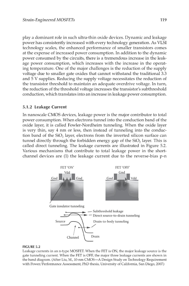
called direct tunneling. The leakage currents are illustrated in Figure 5.2.
Various mechanisms that contribute to total leakage power in the shortchannel devices are (1) the leakage current due to the reverse-bias p-n
Gate insulator tunneling
Gnd
Gnd
Vdd
FET ‘ON’
Gnd
Gnd
Vdd
FET ‘OFF’
Source
Channel
Drain
Subthreshold leakage
Direct source-to-drain tunneling
Drain-to-body tunneling
FIGURE 5.2
Leakage currents in an n-type MOSFET. When the FET is ON, the major leakage source is the
gate tunneling current. When the FET is OFF, the major three leakage currents are shown in
the band diagram. (After Liu, M., 10-nm CMOS—A Design Study on Technology Requirement
with Power/Performance Assessment, PhD thesis, University of California, San Diego, 2007.)
Strain-Engineered MOSFETs
play a dominant role in such ultra-thin oxide devices. Dynamic and leakage
power has consistently increased with every technology generation. As VLSI
technology scales, the enhanced performance of smaller transistors comes
at the expense of increased power consumption. In addition to the dynamic
power consumed by the circuits, there is a tremendous increase in the leakage power consumption, which increases with the increase in the operating temperature. One of the major challenges is the reduction of the supply
voltage due to smaller gate oxides that cannot withstand the traditional 3.3
and 5 V supplies. Reducing the supply voltage necessitates the reduction of
the transistor threshold to maintain an adequate overdrive voltage. In turn,
the reduction of the threshold voltage increases the transistor’s subthreshold
conduction, which translates into an increase in leakage power consumption.
5.1.2 Leakage Current
In nanoscale CMOS devices, leakage power is the major contributor to total
power consumption. When electrons tunnel into the conduction band of the
oxide layer, it is called Fowler-Nordheim tunneling. When the oxide layer
is very thin, say 4 nm or less, then instead of tunneling into the conduction band of the SiO 2 layer, electrons from the inverted silicon surface can
tunnel directly through the forbidden energy gap of the SiO 2 layer. This is
called direct tunneling. The leakage currents are illustrated in Figure 5.2.
Various mechanisms that contribute to total leakage power in the shortchannel devices are (1) the leakage current due to the reverse-bias p-n
Gate insulator tunneling
Gnd
Gnd
Vdd
FET ‘ON’
Gnd
Gnd
Vdd
FET ‘OFF’
Source
Channel
Drain
Subthreshold leakage
Direct source-to-drain tunneling
Drain-to-body tunneling
FIGURE 5.2
Leakage currents in an n-type MOSFET. When the FET is ON, the major leakage source is the
gate tunneling current. When the FET is OFF, the major three leakage currents are shown in
the band diagram. (After Liu, M., 10-nm CMOS—A Design Study on Technology Requirement
with Power/Performance Assessment, PhD thesis, University of California, San Diego, 2007.)