

116
Strain-Engineered MOSFETs
scaling capability of planar bulk or silicon-on-insulator (SOI) MOSFETs. The
three primary SCEs are:
1. V th roll-off: A portion of the channel is already depleted, and hence the
gate electrode does not have to alter the potential at the dielectric interface near the source/drain junction as much to invert the channel V th .
2. S/D off-state leakage: As the depletion width increases further
into the body/channel area, a large V ds results in carriers traversing
through the body rather than the channel from source to drain, a
phenomenon commonly referred to as punch-through I off increases.
3. DIBL: As the drain bias is increased to ensure velocity saturation of
carriers in the channel, the depletion region near the drain electrode
creeps further into the channel and undermines or replaces gate
control of the transistor, with drain control I d becoming independent
of V g .
As channel length is scaled down, the performance is expected to increase
as a result of the decrease in the intrinsic channel resistance. However, the
extrinsic series resistance does not scale proportionately and is becoming a
significant part of the total device resistance.
To overcome these problems, new device architectures as well as new gate
stacks are being investigated. Multigate (also known as FinFET) devices are
considered a promising architecture for replacement of conventional planar MOSFET devices, offering a solution for overcoming the short-channel
effects and providing better V th control at short gate lengths. The nonplanar
10
0
10
–1
Micron
10
–2
1990
1995
2000
Year
2005
2010
Transistor
physical gate
length
Technology
node
70 nm
50 nm
30 nm
15 nm
45 nm
65 nm
90 nm
0.13 µm
0.18 µm
0.25 µm
0.35 µm
0.5 µm
130 nm
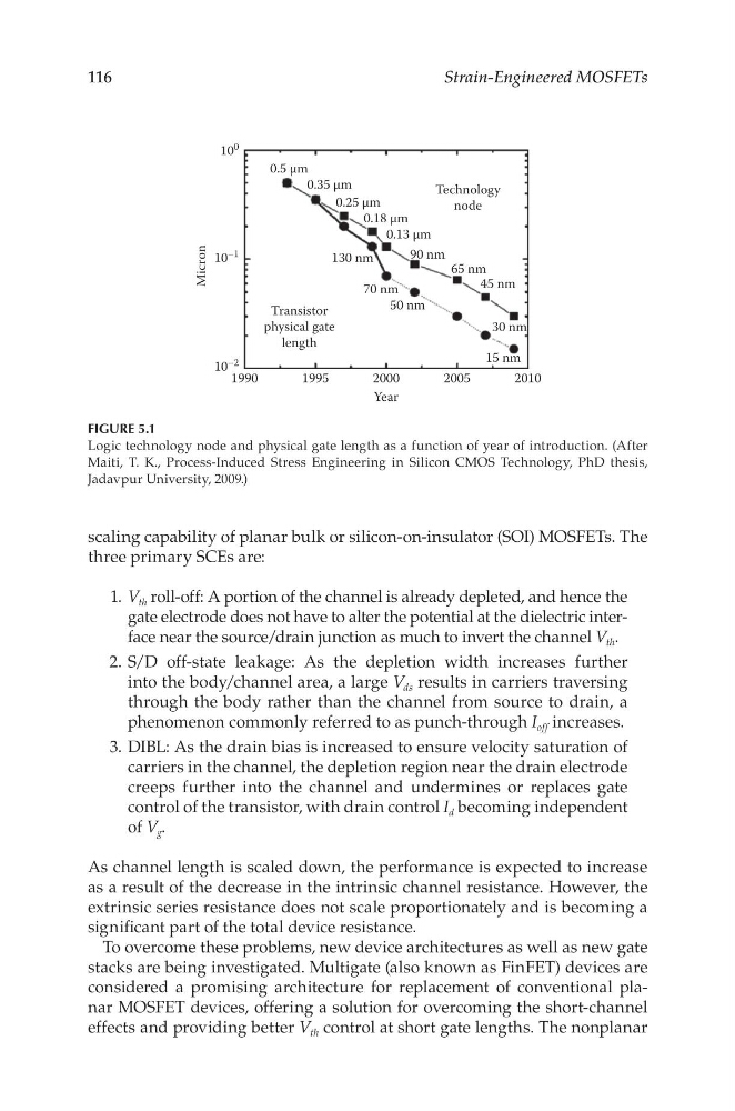
FIGURE 5.1
Logic technology node and physical gate length as a function of year of introduction. (After
Maiti, T. K., Process-Induced Stress Engineering in Silicon CMOS Technology, PhD thesis,
Jadavpur University, 2009.)
Strain-Engineered MOSFETs
scaling capability of planar bulk or silicon-on-insulator (SOI) MOSFETs. The
three primary SCEs are:
1. V th roll-off: A portion of the channel is already depleted, and hence the
gate electrode does not have to alter the potential at the dielectric interface near the source/drain junction as much to invert the channel V th .
2. S/D off-state leakage: As the depletion width increases further
into the body/channel area, a large V ds results in carriers traversing
through the body rather than the channel from source to drain, a
phenomenon commonly referred to as punch-through I off increases.
3. DIBL: As the drain bias is increased to ensure velocity saturation of
carriers in the channel, the depletion region near the drain electrode
creeps further into the channel and undermines or replaces gate
control of the transistor, with drain control I d becoming independent
of V g .
As channel length is scaled down, the performance is expected to increase
as a result of the decrease in the intrinsic channel resistance. However, the
extrinsic series resistance does not scale proportionately and is becoming a
significant part of the total device resistance.
To overcome these problems, new device architectures as well as new gate
stacks are being investigated. Multigate (also known as FinFET) devices are
considered a promising architecture for replacement of conventional planar MOSFET devices, offering a solution for overcoming the short-channel
effects and providing better V th control at short gate lengths. The nonplanar
10
0
10
–1
Micron
10
–2
1990
1995
2000
Year
2005
2010
Transistor
physical gate
length
Technology
node
70 nm
50 nm
30 nm
15 nm
45 nm
65 nm
90 nm
0.13 µm
0.18 µm
0.25 µm
0.35 µm
0.5 µm
130 nm
FIGURE 5.1
Logic technology node and physical gate length as a function of year of introduction. (After
Maiti, T. K., Process-Induced Stress Engineering in Silicon CMOS Technology, PhD thesis,
Jadavpur University, 2009.)