

111
Electronic Properties of Strain-Engineered Semiconductors
4.11 Summary
Stress–strain engineering is now a key performance booster for CMOS
devices. Mechanical stress can affect band gap, effective mass, and carrier
mobility. The band structure of strained Si considering spin-orbit coupling
and the k.p method has been considered to get a deeper understanding
about the energy band. The piezoresistance mobility model, stress-induced
mobility model, and deformation potential-based electron/hole-phonon
interaction-based mobility model have been developed. Procedures for
implementing the models in Sentaurus Device have been described in detail.
Review Questions
1. What is mobility scaling?
2. What is a piezoresistive model?
3. What is a valence band offset in SiGe?
4. What is a conduction band offset in SiGe?
5. What is type II band alignment?
6. What are heavy- and light-hole bands?
7. How can band structures be modified by applied stress?
8. What is the role of acoustic phonons on mobility?
140
120
100
Mobility (cm 2
V –1
S –1
)
80
60
40
0.2
0.4
0.6
E EFF (MV/cm)
0.8
1.0
(100)
(110)
Rim et al.
2002
Rim et
al. 1995
Universal hole
mobility
ompson et al.
2004
1.2
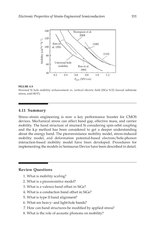
FIGURE 4.9
Strained Si hole mobility enhancement vs. vertical electric field (SiGe S/D, biaxial substrate
stress, and HOT).
Electronic Properties of Strain-Engineered Semiconductors
4.11 Summary
Stress–strain engineering is now a key performance booster for CMOS
devices. Mechanical stress can affect band gap, effective mass, and carrier
mobility. The band structure of strained Si considering spin-orbit coupling
and the k.p method has been considered to get a deeper understanding
about the energy band. The piezoresistance mobility model, stress-induced
mobility model, and deformation potential-based electron/hole-phonon
interaction-based mobility model have been developed. Procedures for
implementing the models in Sentaurus Device have been described in detail.
Review Questions
1. What is mobility scaling?
2. What is a piezoresistive model?
3. What is a valence band offset in SiGe?
4. What is a conduction band offset in SiGe?
5. What is type II band alignment?
6. What are heavy- and light-hole bands?
7. How can band structures be modified by applied stress?
8. What is the role of acoustic phonons on mobility?
140
120
100
Mobility (cm 2
V –1
S –1
)
80
60
40
0.2
0.4
0.6
E EFF (MV/cm)
0.8
1.0
(100)
(110)
Rim et al.
2002
Rim et
al. 1995
Universal hole
mobility
ompson et al.
2004
1.2
FIGURE 4.9
Strained Si hole mobility enhancement vs. vertical electric field (SiGe S/D, biaxial substrate
stress, and HOT).