

110
Strain-Engineered MOSFETs
2
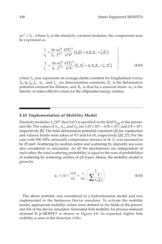
v S ij
ρ = , where S ij is the elasticity constant modulus, the components may
be expressed as
1 3
2
1 3
2
3/2
3/2
1/2
2 4
2
2
3/2
3/2
1/2
2 4
2
2
S
m kTE
S
m kTE
ii
D
k
d
d u
u
ii
D
k
d
d u
u
(
)
(
)
τ
=
π
π
ξ Ξ + η Ξ Ξ + ζ Ξ
τ
=
π
π
ξ Ξ + η Ξ Ξ + ζ Ξ
⊥
⊥
⊥
⊥
(4.60)
where S ii now represents an average elastic constant for longitudinal waves;
, , , ,
ξ η ζ ξ η
⊥
⊥ , and ζ ⊥ are dimensionless constants; d
Ξ is the deformation
potential constant for dilation; and u
Ξ is that for a uniaxial strain. m D is the
density of states effective mass for the ellipsoidal energy surface.
4.10 Implementation of Mobility Model
Elasticity modulus S ij (10 12 dyn/cm 2 ) is specified in the field S [i][j] in the parameter file. The values of S 11 , S 12 , and S 44 are 1.23 × 10 12 , –4.76 × 10 12 , and 0.8 × 10 12 ,
respectively [8]. The total deformation potential constants (Ξ) for conduction
and valance bands were taken as 9.5 and 6.6 eV, respectively [20, 27]. For the
case with 500 MPa uniaxially compressive stresses in Si, E k was assumed to
be 25 meV. Scattering by neutral centre and scattering by impurity ion were
also considered in simulation. As all the mechanisms are independent of
each other, the total scattering probability is equal to the sum of probabilities
of scattering by scattering centres of all types. Hence, the mobility model is
given by
1
1
( )
*
*
e
m
e
m
E
r
D
D
i
∑
µ = 〈τ〉 =
〈τ〉 =
τ
(4.61)
The above mobility was considered in a hydrodynamic model and was
implemented in the Sentaurus Device simulator. To activate the mobility
model, appropriate mobility values were defined in the fields of the parameter file of the device simulator. Simulated hole mobility for process-induced
strained Si p-MOSFET is shown in Figure 4.9. As expected, higher hole
mobility is seen in the direction <110>.
Strain-Engineered MOSFETs
2
v S ij
ρ = , where S ij is the elasticity constant modulus, the components may
be expressed as
1 3
2
1 3
2
3/2
3/2
1/2
2 4
2
2
3/2
3/2
1/2
2 4
2
2
S
m kTE
S
m kTE
ii
D
k
d
d u
u
ii
D
k
d
d u
u
(
)
(
)
τ
=
π
π
ξ Ξ + η Ξ Ξ + ζ Ξ
τ
=
π
π
ξ Ξ + η Ξ Ξ + ζ Ξ
⊥
⊥
⊥
⊥
(4.60)
where S ii now represents an average elastic constant for longitudinal waves;
, , , ,
ξ η ζ ξ η
⊥
⊥ , and ζ ⊥ are dimensionless constants; d
Ξ is the deformation
potential constant for dilation; and u
Ξ is that for a uniaxial strain. m D is the
density of states effective mass for the ellipsoidal energy surface.
4.10 Implementation of Mobility Model
Elasticity modulus S ij (10 12 dyn/cm 2 ) is specified in the field S [i][j] in the parameter file. The values of S 11 , S 12 , and S 44 are 1.23 × 10 12 , –4.76 × 10 12 , and 0.8 × 10 12 ,
respectively [8]. The total deformation potential constants (Ξ) for conduction
and valance bands were taken as 9.5 and 6.6 eV, respectively [20, 27]. For the
case with 500 MPa uniaxially compressive stresses in Si, E k was assumed to
be 25 meV. Scattering by neutral centre and scattering by impurity ion were
also considered in simulation. As all the mechanisms are independent of
each other, the total scattering probability is equal to the sum of probabilities
of scattering by scattering centres of all types. Hence, the mobility model is
given by
1
1
( )
*
*
e
m
e
m
E
r
D
D
i
∑
µ = 〈τ〉 =
〈τ〉 =
τ
(4.61)
The above mobility was considered in a hydrodynamic model and was
implemented in the Sentaurus Device simulator. To activate the mobility
model, appropriate mobility values were defined in the fields of the parameter file of the device simulator. Simulated hole mobility for process-induced
strained Si p-MOSFET is shown in Figure 4.9. As expected, higher hole
mobility is seen in the direction <110>.