

102
Strain-Engineered MOSFETs
of ( , )
P N T
α
is based on an analytic fit of the Fermi integrals [32]. Finally, the
expression for piezoresistive coefficients is given by
.
300
( / )
( / )
,
, var
(1/2)
(1/2)
T
F
E k T
F
E k T
ij
ij kon
ij
s
F
B
s
F
B
π = π
+π
′ +
+
(4.27)
The piezoresistive model is applied in our simulations by including the
name of the model in the subsection of the input command file. The effect
of mechanical stress on the mobility may then be expressed in terms of the
piezoresistive coefficient as follows:
|| ||
µ
µ
≈ π σ + π σ
⊥ ⊥
(4.28)
Using Equation (4.28), we have computed the mobility and subsequently
simulated the MOSFET device characteristics. When dealing with the simulation of stress effect in silicon, there are three coordinate systems: the crystal
system, the simulation system, and the stress system. Miller indices are used
to describe the orientation of one system with respect to another. The simulation system with respect to the crystal system was defined in the parameter
file.par in the LatticeParameter section, the default orientation
of the simulation system. For the <110> channel direction in CMOS, the following parameter is used in the.par file [8].
LatticeParameters {
X = (1, 0, 1)
Y = (0, 1, 0)}
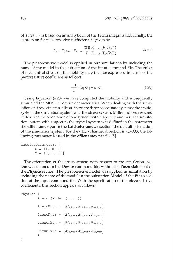
The orientation of the stress system with respect to the simulation system was defined in the Device command file, within the Piezo statement of
the Physics section. The piezoresistive model was applied in simulation by
including the name of the model in the subsection Model of the Piezo section of the input command file. With the specification of the piezoresistive
coefficients, this section appears as follows:
Physics {
Piezo (Model (……………))
PiezoNkon =
kon
n
kon
n
kon
n
,
,
11,
1 2,
44,
(
)
π
π
π
PiezoNvar =
n
n
n
,
,
11,var
12,var
44,var
(
)
π
π
π
PiezoPkon =
kon
p
kon
p
kon
p
,
,
11,
1 2,
44,
(
)
π
π
π
PiezoPvar =
p
p
p
,
,
11,var
12,var
44,var
(
)
π
π
π
)
}
Strain-Engineered MOSFETs
of ( , )
P N T
α
is based on an analytic fit of the Fermi integrals [32]. Finally, the
expression for piezoresistive coefficients is given by
.
300
( / )
( / )
,
, var
(1/2)
(1/2)
T
F
E k T
F
E k T
ij
ij kon
ij
s
F
B
s
F
B
π = π
+π
′ +
+
(4.27)
The piezoresistive model is applied in our simulations by including the
name of the model in the subsection of the input command file. The effect
of mechanical stress on the mobility may then be expressed in terms of the
piezoresistive coefficient as follows:
|| ||
µ
µ
≈ π σ + π σ
⊥ ⊥
(4.28)
Using Equation (4.28), we have computed the mobility and subsequently
simulated the MOSFET device characteristics. When dealing with the simulation of stress effect in silicon, there are three coordinate systems: the crystal
system, the simulation system, and the stress system. Miller indices are used
to describe the orientation of one system with respect to another. The simulation system with respect to the crystal system was defined in the parameter
file
of the simulation system. For the <110> channel direction in CMOS, the following parameter is used in the
LatticeParameters {
X = (1, 0, 1)
Y = (0, 1, 0)}
The orientation of the stress system with respect to the simulation system was defined in the Device command file, within the Piezo statement of
the Physics section. The piezoresistive model was applied in simulation by
including the name of the model in the subsection Model of the Piezo section of the input command file. With the specification of the piezoresistive
coefficients, this section appears as follows:
Physics {
Piezo (Model (……………))
PiezoNkon =
kon
n
kon
n
kon
n
,
,
11,
1 2,
44,
(
)
π
π
π
PiezoNvar =
n
n
n
,
,
11,var
12,var
44,var
(
)
π
π
π
PiezoPkon =
kon
p
kon
p
kon
p
,
,
11,
1 2,
44,
(
)
π
π
π
PiezoPvar =
p
p
p
,
,
11,var
12,var
44,var
(
)
π
π
π
)
}