

101
Electronic Properties of Strain-Engineered Semiconductors
where e is the electron charge, and
( , ˆ )/
1
v
kX k
i
i
=
∂ε
∂
−
is the ith component
of the group velocity of charge carriers. The change in conductivity under
stress is given by
4
( ) ( )
2
3
0
e
f
v v k
ij
i j
∫
σ = − Π
∂ ε
∂ε
τ ε
δ
(4.23)
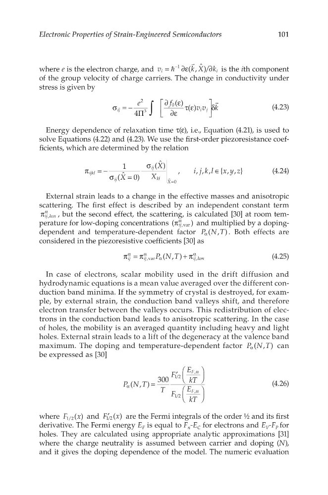
Energy dependence of relaxation time τ(ε), i.e., Equation (4.21), is used to
solve Equations (4.22) and (4.23). We use the first-order piezoresistance coefficients, which are determined by the relation
1
( ˆ 0)
( ˆ )
,
, , , { , , }
ˆ 0
X
X
X
i j k l x y z
ijkl
ij
ij
kl
X
π = − σ
=
σ
∈
=
(4.24)
External strain leads to a change in the effective masses and anisotropic
scattering. The first effect is described by an independent constant term
,
ij kon
π
α
, but the second effect, the scattering, is calculated [30] at room temperature for low-doping concentrations (
)
,var
ij
π
α
and multiplied by a dopingdependent and temperature-dependent factor
( , )
P N T
α
. Both effects are
considered in the piezoresistive coefficients [30] as
( , )
,var
,
P N T
ij
ij
ij kon
π = π
+ π
α
α
α
α
(4.25)
In case of electrons, scalar mobility used in the drift diffusion and
hydrodynamic equations is a mean value averaged over the different conduction band minima. If the symmetry of crystal is destroyed, for example, by external strain, the conduction band valleys shift, and therefore
electron transfer between the valleys occurs. This redistribution of electrons in the conduction band leads to anisotropic scattering. In the case
of holes, the mobility is an averaged quantity including heavy and light
holes. External strain leads to a lift of the degeneracy at the valence band
maximum. The doping and temperature-dependent factor
( , )
P N T
α
can
be expressed as [30]
( , )
300
1/2
,
1/2
,
P N T
T
F
E
kT
F
E
kT
F
F
=
′
α
α
α
(4.26)
where
( )
1/2
F x and
( )
1/2
F x
′
are the Fermi integrals of the order ½ and its first
derivative. The Fermi energy E F is equal to F n -E C for electrons and E V -F P for
holes. They are calculated using appropriate analytic approximations [31]
where the charge neutrality is assumed between carrier and doping (N),
and it gives the doping dependence of the model. The numeric evaluation
Electronic Properties of Strain-Engineered Semiconductors
where e is the electron charge, and
( , ˆ )/
1
v
kX k
i
i
=
∂ε
∂
−
is the ith component
of the group velocity of charge carriers. The change in conductivity under
stress is given by
4
( ) ( )
2
3
0
e
f
v v k
ij
i j
∫
σ = − Π
∂ ε
∂ε
τ ε
δ
(4.23)
Energy dependence of relaxation time τ(ε), i.e., Equation (4.21), is used to
solve Equations (4.22) and (4.23). We use the first-order piezoresistance coefficients, which are determined by the relation
1
( ˆ 0)
( ˆ )
,
, , , { , , }
ˆ 0
X
X
X
i j k l x y z
ijkl
ij
ij
kl
X
π = − σ
=
σ
∈
=
(4.24)
External strain leads to a change in the effective masses and anisotropic
scattering. The first effect is described by an independent constant term
,
ij kon
π
α
, but the second effect, the scattering, is calculated [30] at room temperature for low-doping concentrations (
)
,var
ij
π
α
and multiplied by a dopingdependent and temperature-dependent factor
( , )
P N T
α
. Both effects are
considered in the piezoresistive coefficients [30] as
( , )
,var
,
P N T
ij
ij
ij kon
π = π
+ π
α
α
α
α
(4.25)
In case of electrons, scalar mobility used in the drift diffusion and
hydrodynamic equations is a mean value averaged over the different conduction band minima. If the symmetry of crystal is destroyed, for example, by external strain, the conduction band valleys shift, and therefore
electron transfer between the valleys occurs. This redistribution of electrons in the conduction band leads to anisotropic scattering. In the case
of holes, the mobility is an averaged quantity including heavy and light
holes. External strain leads to a lift of the degeneracy at the valence band
maximum. The doping and temperature-dependent factor
( , )
P N T
α
can
be expressed as [30]
( , )
300
1/2
,
1/2
,
P N T
T
F
E
kT
F
E
kT
F
F
=
′
α
α
α
(4.26)
where
( )
1/2
F x and
( )
1/2
F x
′
are the Fermi integrals of the order ½ and its first
derivative. The Fermi energy E F is equal to F n -E C for electrons and E V -F P for
holes. They are calculated using appropriate analytic approximations [31]
where the charge neutrality is assumed between carrier and doping (N),
and it gives the doping dependence of the model. The numeric evaluation