

103
Electronic Properties of Strain-Engineered Semiconductors
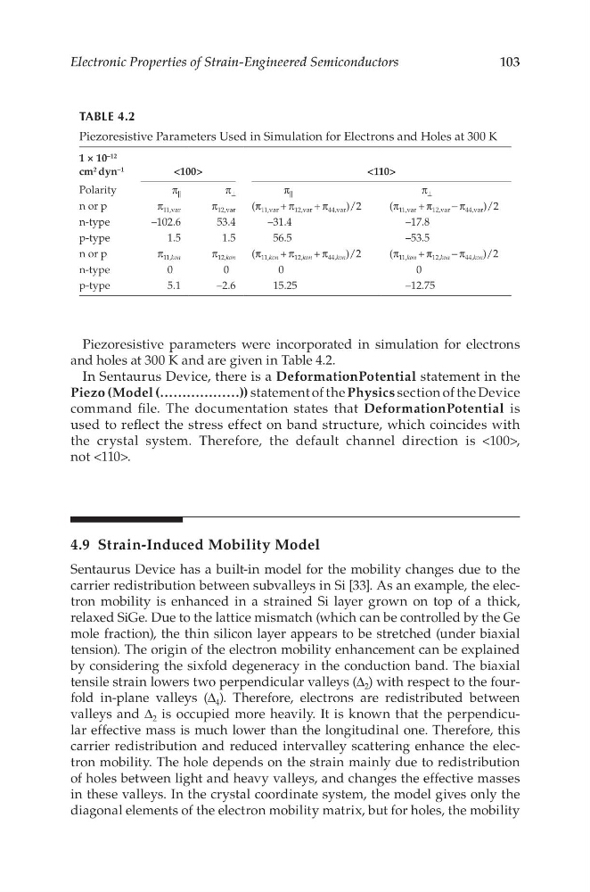
Piezoresistive parameters were incorporated in simulation for electrons
and holes at 300 K and are given in Table 4.2.
In Sentaurus Device, there is a DeformationPotential statement in the
Piezo (Model (………………)) statement of the Physics section of the Device
command file. The documentation states that DeformationPotential is
used to reflect the stress effect on band structure, which coincides with
the crystal system. Therefore, the default channel direction is <100>,
not <110>.
4.9 Strain-Induced Mobility Model
Sentaurus Device has a built-in model for the mobility changes due to the
carrier redistribution between subvalleys in Si [33]. As an example, the electron mobility is enhanced in a strained Si layer grown on top of a thick,
relaxed SiGe. Due to the lattice mismatch (which can be controlled by the Ge
mole fraction), the thin silicon layer appears to be stretched (under biaxial
tension). The origin of the electron mobility enhancement can be explained
by considering the sixfold degeneracy in the conduction band. The biaxial
tensile strain lowers two perpendicular valleys (Δ 2 ) with respect to the fourfold in-plane valleys (Δ 4 ). Therefore, electrons are redistributed between
valleys and Δ 2 is occupied more heavily. It is known that the perpendicular effective mass is much lower than the longitudinal one. Therefore, this
carrier redistribution and reduced intervalley scattering enhance the electron mobility. The hole depends on the strain mainly due to redistribution
of holes between light and heavy valleys, and changes the effective masses
in these valleys. In the crystal coordinate system, the model gives only the
diagonal elements of the electron mobility matrix, but for holes, the mobility
TABLE 4.2
Piezoresistive Parameters Used in Simulation for Electrons and Holes at 300 K
1 × 10 –12
cm 2 dyn –1
<100>
<110>
Polarity
π ||
π ⊥
π ||
π ⊥
n or p
π 11,var
π 12,var (π 11,var + π 12,var + π 44,var )/2
(π 11,var + π 12,var − π 44,var )/2
n-type
–102.6
53.4
–31.4
–17.8
p-type
1.5
1.5
56.5
–53.5
n or p
π 11,kon
π 12,kon (π 11,kon + π 12,kon + π 44,kon )/2
(π 11,kon + π 12,kon − π 44,kon )/2
n-type
0
0
0
0
p-type
5.1
–2.6
15.25
–12.75
Electronic Properties of Strain-Engineered Semiconductors
Piezoresistive parameters were incorporated in simulation for electrons
and holes at 300 K and are given in Table 4.2.
In Sentaurus Device, there is a DeformationPotential statement in the
Piezo (Model (………………)) statement of the Physics section of the Device
command file. The documentation states that DeformationPotential is
used to reflect the stress effect on band structure, which coincides with
the crystal system. Therefore, the default channel direction is <100>,
not <110>.
4.9 Strain-Induced Mobility Model
Sentaurus Device has a built-in model for the mobility changes due to the
carrier redistribution between subvalleys in Si [33]. As an example, the electron mobility is enhanced in a strained Si layer grown on top of a thick,
relaxed SiGe. Due to the lattice mismatch (which can be controlled by the Ge
mole fraction), the thin silicon layer appears to be stretched (under biaxial
tension). The origin of the electron mobility enhancement can be explained
by considering the sixfold degeneracy in the conduction band. The biaxial
tensile strain lowers two perpendicular valleys (Δ 2 ) with respect to the fourfold in-plane valleys (Δ 4 ). Therefore, electrons are redistributed between
valleys and Δ 2 is occupied more heavily. It is known that the perpendicular effective mass is much lower than the longitudinal one. Therefore, this
carrier redistribution and reduced intervalley scattering enhance the electron mobility. The hole depends on the strain mainly due to redistribution
of holes between light and heavy valleys, and changes the effective masses
in these valleys. In the crystal coordinate system, the model gives only the
diagonal elements of the electron mobility matrix, but for holes, the mobility
TABLE 4.2
Piezoresistive Parameters Used in Simulation for Electrons and Holes at 300 K
1 × 10 –12
cm 2 dyn –1
<100>
<110>
Polarity
π ||
π ⊥
π ||
π ⊥
n or p
π 11,var
π 12,var (π 11,var + π 12,var + π 44,var )/2
(π 11,var + π 12,var − π 44,var )/2
n-type
–102.6
53.4
–31.4
–17.8
p-type
1.5
1.5
56.5
–53.5
n or p
π 11,kon
π 12,kon (π 11,kon + π 12,kon + π 44,kon )/2
(π 11,kon + π 12,kon − π 44,kon )/2
n-type
0
0
0
0
p-type
5.1
–2.6
15.25
–12.75