

Furthermore, the escape depth of the higher-energy photoelectrons is larger,
allowing a good approximation to bulk sensitivity. As documented in
Appendix K, there are now more than 24 HAXPES beamlines in operation or
under construction around the world.
How deep can HAXPS probe? For some samples, it is useful to employ an
“information depth,” defined by Kobayashi as the thickness of the layer from
which 90% of the photoelectron signal originates [528]. But for buried interfaces,
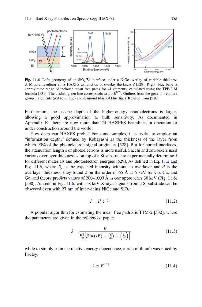
the attenuation length λ of photoelectrons is more useful. Sacchi and coworkers used
various overlayer thicknesses on top of a Si substrate to experimentally determine λ
for different materials and photoelectron energies [529]. As defined in Eq. 11.2 and
Fig. 11.6, where I
s
0 is the expected intensity without an overlayer and d is the
overlayer thickness, they found λ on the order of 65 Å at 6 keV for Co, Cu, and
Ge, and theory predicts values of 200–1000 Å as one approaches 30 keV (Fig. 11.6)
[530]. As seen in Fig. 11.6, with ~8 keV X-rays, signals from a Si substrate can be
observed even with 27 nm of intervening NiGe and SiO 2 :
I ¼ I
s
0 e
À
d
λ
ð11:2Þ
A popular algorithm for estimating the mean free path λ is TTM-2 [532], where
the parameters are given in the referenced paper:
λ ¼
E
E
2
p β ln γE
ð Þ À
C
E
À Á þ
D
E
2
h
i
ð11:3Þ
while to simply estimate relative energy dependence, a rule of thumb was noted by
Fadley:
λ / E
0:78
ð11:4Þ
Fig. 11.6 Left: geometry of an SiO 2 /Si interface under a NiGe overlay of variable thickness
d. Middle: resulting Si 1s HAXPS as function of overlay thickness d [528]. Right: blue band is
approximate range of inelastic mean free paths for 41 elements, calculated using the TPP-2 M
formula [531]. The dashed green line corresponds to λ /E
0.78
. Outliers from the general trend are
group 1 elements (red solid line) and diamond (dashed blue line). Revised from [516]
11.3 Hard X-ray Photoelectron Spectroscopy (HAXPS)
285
allowing a good approximation to bulk sensitivity. As documented in
Appendix K, there are now more than 24 HAXPES beamlines in operation or
under construction around the world.
How deep can HAXPS probe? For some samples, it is useful to employ an
“information depth,” defined by Kobayashi as the thickness of the layer from
which 90% of the photoelectron signal originates [528]. But for buried interfaces,
the attenuation length λ of photoelectrons is more useful. Sacchi and coworkers used
various overlayer thicknesses on top of a Si substrate to experimentally determine λ
for different materials and photoelectron energies [529]. As defined in Eq. 11.2 and
Fig. 11.6, where I
s
0 is the expected intensity without an overlayer and d is the
overlayer thickness, they found λ on the order of 65 Å at 6 keV for Co, Cu, and
Ge, and theory predicts values of 200–1000 Å as one approaches 30 keV (Fig. 11.6)
[530]. As seen in Fig. 11.6, with ~8 keV X-rays, signals from a Si substrate can be
observed even with 27 nm of intervening NiGe and SiO 2 :
I ¼ I
s
0 e
À
d
λ
ð11:2Þ
A popular algorithm for estimating the mean free path λ is TTM-2 [532], where
the parameters are given in the referenced paper:
λ ¼
E
E
2
p β ln γE
ð Þ À
C
E
À Á þ
D
E
2
h
i
ð11:3Þ
while to simply estimate relative energy dependence, a rule of thumb was noted by
Fadley:
λ / E
0:78
ð11:4Þ
Fig. 11.6 Left: geometry of an SiO 2 /Si interface under a NiGe overlay of variable thickness
d. Middle: resulting Si 1s HAXPS as function of overlay thickness d [528]. Right: blue band is
approximate range of inelastic mean free paths for 41 elements, calculated using the TPP-2 M
formula [531]. The dashed green line corresponds to λ /E
0.78
. Outliers from the general trend are
group 1 elements (red solid line) and diamond (dashed blue line). Revised from [516]
11.3 Hard X-ray Photoelectron Spectroscopy (HAXPS)
285