

5.6 Charge-Coupled Devices (CCDs)
Charge-coupled devices or “CCDs” are in every home with a digital camera. They
are lithographically produced by two-dimensional arrays of photodiodes connected
to form the electronic equivalent of a “bucket brigade” (Fig. 5.6), and the “chargecoupling” refers to this motion of charges between adjacent locations. Boyle and
Smith shared part of the 2009 Nobel Prize in Physics for the invention of an imaging
semiconductor circuit—the CCD sensor.
In some cases, the diode material itself is used to stop the incident X-rays. Since
the front of the CCD has an inert passivation layer as well as polysilicon structures
and metal electrodes, in the soft X-ray region, CCDs are often “back-illuminated,”
with a thinned passivation layer for even better sensitivity.
Instead of window losses, hard X-ray detection often has the opposite problem—
obtaining sufficient stopping power to collect most of the X-rays. Space scientists
have developed 300-micron-thick Si CCDs that have better than 90% efficiency
between 0.5 and 10 keV, but their budgets are of course “astronomical.”
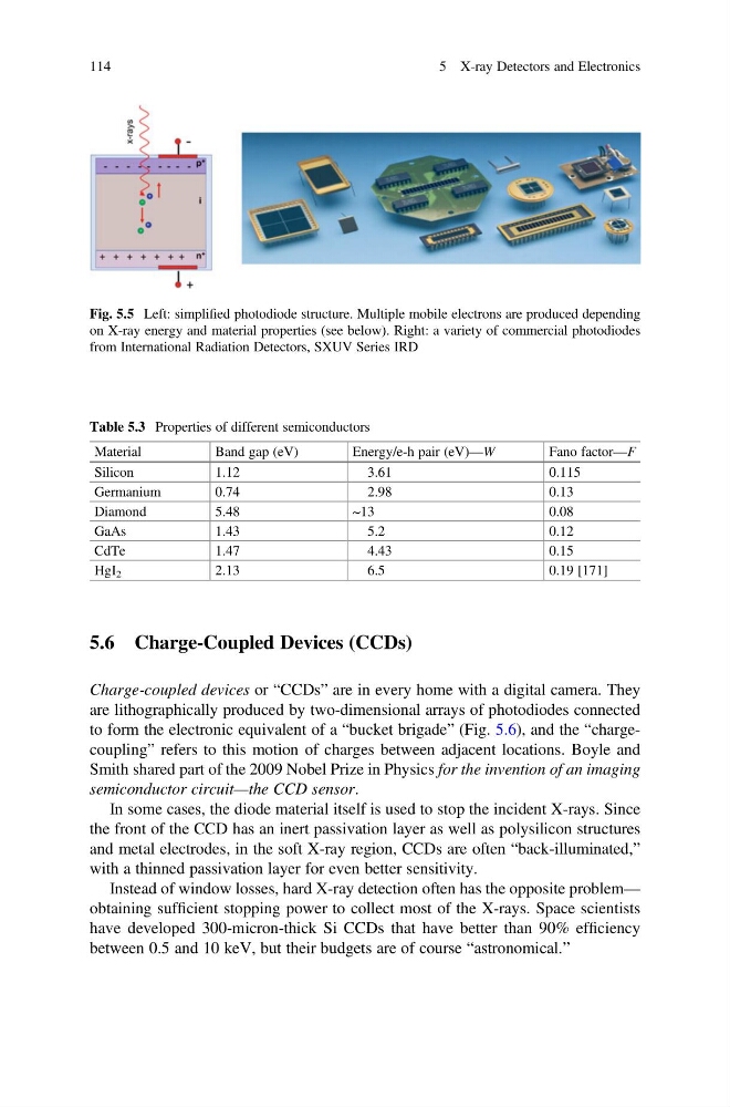
Fig. 5.5 Left: simplified photodiode structure. Multiple mobile electrons are produced depending
on X-ray energy and material properties (see below). Right: a variety of commercial photodiodes
from International Radiation Detectors, SXUV Series IRD
Table 5.3 Properties of different semiconductors
Material
Band gap (eV)
Energy/e-h pair (eV)—W
Fano factor—F
Silicon
1.12
3.61
0.115
Germanium
0.74
2.98
0.13
Diamond
5.48
~13
0.08
GaAs
1.43
5.2
0.12
CdTe
1.47
4.43
0.15
HgI 2
2.13
6.5
0.19 [171]
114
5 X-ray Detectors and Electronics
Charge-coupled devices or “CCDs” are in every home with a digital camera. They
are lithographically produced by two-dimensional arrays of photodiodes connected
to form the electronic equivalent of a “bucket brigade” (Fig. 5.6), and the “chargecoupling” refers to this motion of charges between adjacent locations. Boyle and
Smith shared part of the 2009 Nobel Prize in Physics for the invention of an imaging
semiconductor circuit—the CCD sensor.
In some cases, the diode material itself is used to stop the incident X-rays. Since
the front of the CCD has an inert passivation layer as well as polysilicon structures
and metal electrodes, in the soft X-ray region, CCDs are often “back-illuminated,”
with a thinned passivation layer for even better sensitivity.
Instead of window losses, hard X-ray detection often has the opposite problem—
obtaining sufficient stopping power to collect most of the X-rays. Space scientists
have developed 300-micron-thick Si CCDs that have better than 90% efficiency
between 0.5 and 10 keV, but their budgets are of course “astronomical.”
Fig. 5.5 Left: simplified photodiode structure. Multiple mobile electrons are produced depending
on X-ray energy and material properties (see below). Right: a variety of commercial photodiodes
from International Radiation Detectors, SXUV Series IRD
Table 5.3 Properties of different semiconductors
Material
Band gap (eV)
Energy/e-h pair (eV)—W
Fano factor—F
Silicon
1.12
3.61
0.115
Germanium
0.74
2.98
0.13
Diamond
5.48
~13
0.08
GaAs
1.43
5.2
0.12
CdTe
1.47
4.43
0.15
HgI 2
2.13
6.5
0.19 [171]
114
5 X-ray Detectors and Electronics