

Nanostructured P3HT films with uniform molecular orientation show great
potential for device application. Hu and coworkers reported the manufacture of
OFETs and solar cells on the basis of P3HT nanogratings and observed enhanced
device performance as a result of 3D chain alignment in the nanogratings [126]. For
π-stacking along the grating and a vertical chain orientation [97], in-plane charge
transport in OFETs is greatly enhanced along the grating direction and hence along
the π-stacking (b-axis). Charge carrier mobilities of more than two orders of
magnitude lower are found in the perpendicular direction (i.e., side chain direction,
a-axis), demonstrating a significant charge transport anisotropy in the a-b-plane.
Improved power conversion efficiencies for solar cells based on PCBM and P3HT
nanogratings were found compared with bilayer and blend devices of the same
material, which further depicts the increased order and interfacial area in the highly
ordered P3HT nanostructures. Promising results have also been achieved for
patterned solar cells prepared by solvent vapor-assisted imprint lithography
[127–129].
Despite the power of NIL, there are further methods for obtaining highly ordered
micro- or nanostructures. For example, we made use of a combination of templatedirected dewetting and solvent vapor annealing to produce micrometer-sized P3HT
structures of high order (Fig. 27) [130]. At first, solvent vapor-induced dewetting
from topographically and chemically patterned transistor substrates allowed confining a fluid P3HT film into the micrometer-sized channels of a transistor. Recrystallization in confinement in controlled solvent vapor atmosphere permits low
nucleation densities, leading to the oriented growth of the crystalline lamellae
along the confining channel walls (see case A in Fig. 27). In this molecular
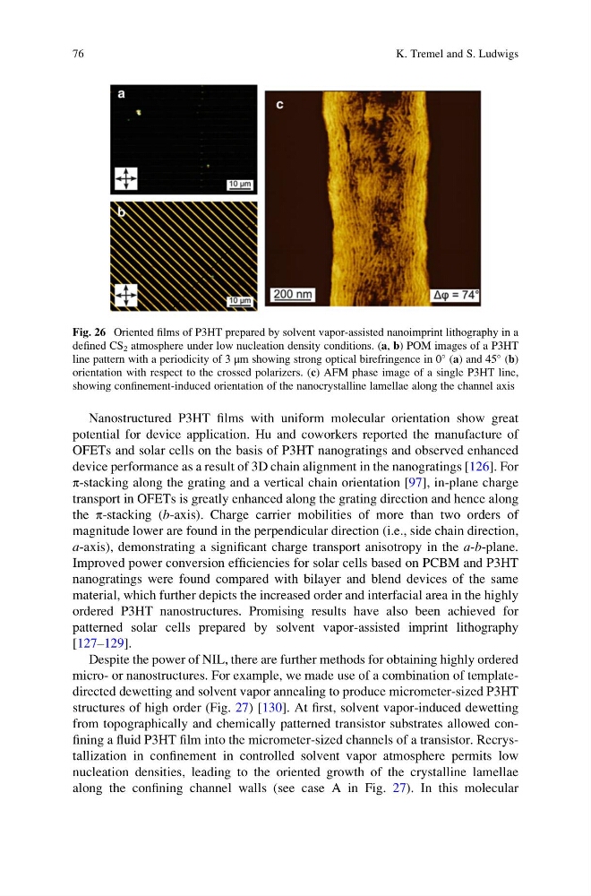
Fig. 26 Oriented films of P3HT prepared by solvent vapor-assisted nanoimprint lithography in a
defined CS 2 atmosphere under low nucleation density conditions. (a, b) POM images of a P3HT
line pattern with a periodicity of 3 μm showing strong optical birefringence in 0
(a) and 45
(b)
orientation with respect to the crossed polarizers. (c) AFM phase image of a single P3HT line,
showing confinement-induced orientation of the nanocrystalline lamellae along the channel axis
76
K. Tremel and S. Ludwigs
potential for device application. Hu and coworkers reported the manufacture of
OFETs and solar cells on the basis of P3HT nanogratings and observed enhanced
device performance as a result of 3D chain alignment in the nanogratings [126]. For
π-stacking along the grating and a vertical chain orientation [97], in-plane charge
transport in OFETs is greatly enhanced along the grating direction and hence along
the π-stacking (b-axis). Charge carrier mobilities of more than two orders of
magnitude lower are found in the perpendicular direction (i.e., side chain direction,
a-axis), demonstrating a significant charge transport anisotropy in the a-b-plane.
Improved power conversion efficiencies for solar cells based on PCBM and P3HT
nanogratings were found compared with bilayer and blend devices of the same
material, which further depicts the increased order and interfacial area in the highly
ordered P3HT nanostructures. Promising results have also been achieved for
patterned solar cells prepared by solvent vapor-assisted imprint lithography
[127–129].
Despite the power of NIL, there are further methods for obtaining highly ordered
micro- or nanostructures. For example, we made use of a combination of templatedirected dewetting and solvent vapor annealing to produce micrometer-sized P3HT
structures of high order (Fig. 27) [130]. At first, solvent vapor-induced dewetting
from topographically and chemically patterned transistor substrates allowed confining a fluid P3HT film into the micrometer-sized channels of a transistor. Recrystallization in confinement in controlled solvent vapor atmosphere permits low
nucleation densities, leading to the oriented growth of the crystalline lamellae
along the confining channel walls (see case A in Fig. 27). In this molecular
Fig. 26 Oriented films of P3HT prepared by solvent vapor-assisted nanoimprint lithography in a
defined CS 2 atmosphere under low nucleation density conditions. (a, b) POM images of a P3HT
line pattern with a periodicity of 3 μm showing strong optical birefringence in 0
(a) and 45
(b)
orientation with respect to the crossed polarizers. (c) AFM phase image of a single P3HT line,
showing confinement-induced orientation of the nanocrystalline lamellae along the channel axis
76
K. Tremel and S. Ludwigs