

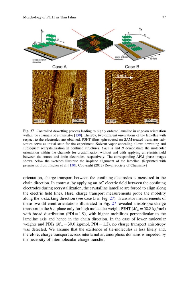
orientation, charge transport between the confining electrodes is measured in the
chain direction. In contrast, by applying an AC electric field between the confining
electrodes during recrystallization, the crystalline lamellae are forced to align along
the electric field lines. Here, charge transport measurements probe the mobility
along the π-stacking direction (see case B in Fig. 27). Transistor measurements of
these two different orientations illustrated in Fig. 27 revealed anisotropic charge
transport in the b-c-plane only for high molecular weight P3HT (M w ¼ 58.8 kg/mol)
with broad distribution (PDI ¼ 1.9), with higher mobilities perpendicular to the
lamellae axis and hence in the chain direction. In the case of lower molecular
weights and PDIs (M w ¼ 30.0 kg/mol, PDI ¼ 1.2), no charge transport anisotropy
was detected. We assume that the existence of tie-molecules is less likely and,
therefore, charge transport across interlamellar, amorphous domains is impeded by
the necessity of intermolecular charge transfer.
Fig. 27 Controlled dewetting process leading to highly ordered lamellae in edge-on orientation
within the channels of a transistor [130]. Thereby, two different orientations of the lamellae with
respect to the electrodes are obtained. P3HT films spin-coated on SAM-treated transistor substrates serve as initial state for the experiment. Solvent vapor annealing allows dewetting and
subsequent recrystallization in confined structures. Case A and B demonstrate the molecular
orientation within the channels for crystallization without and with applying an electric field
between the source and drain electrodes, respectively. The corresponding AFM phase images
shown below the sketches illustrate the in-plane alignment of the lamellae. (Reprinted with
permission from Fischer et al. [130]. Copyright (2012) Royal Society of Chemistry)
Morphology of P3HT in Thin Films
77
chain direction. In contrast, by applying an AC electric field between the confining
electrodes during recrystallization, the crystalline lamellae are forced to align along
the electric field lines. Here, charge transport measurements probe the mobility
along the π-stacking direction (see case B in Fig. 27). Transistor measurements of
these two different orientations illustrated in Fig. 27 revealed anisotropic charge
transport in the b-c-plane only for high molecular weight P3HT (M w ¼ 58.8 kg/mol)
with broad distribution (PDI ¼ 1.9), with higher mobilities perpendicular to the
lamellae axis and hence in the chain direction. In the case of lower molecular
weights and PDIs (M w ¼ 30.0 kg/mol, PDI ¼ 1.2), no charge transport anisotropy
was detected. We assume that the existence of tie-molecules is less likely and,
therefore, charge transport across interlamellar, amorphous domains is impeded by
the necessity of intermolecular charge transfer.
Fig. 27 Controlled dewetting process leading to highly ordered lamellae in edge-on orientation
within the channels of a transistor [130]. Thereby, two different orientations of the lamellae with
respect to the electrodes are obtained. P3HT films spin-coated on SAM-treated transistor substrates serve as initial state for the experiment. Solvent vapor annealing allows dewetting and
subsequent recrystallization in confined structures. Case A and B demonstrate the molecular
orientation within the channels for crystallization without and with applying an electric field
between the source and drain electrodes, respectively. The corresponding AFM phase images
shown below the sketches illustrate the in-plane alignment of the lamellae. (Reprinted with
permission from Fischer et al. [130]. Copyright (2012) Royal Society of Chemistry)
Morphology of P3HT in Thin Films
77