

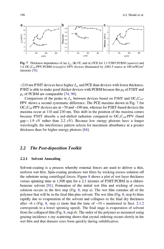
~210 nm P3HT devices have higher J sc and PCE than devices with lower thickness.
P3HT is able to make good thicker devices with PCBM because the μ h of P3HT and
μ e of PCBM are comparable [74, 90].
Comparison of the peaks in J sc between devices based on P3HT and OC 1 C 10 -
PPV shows a second systematic difference. The PCE maxima shown in Fig. 7 for
OC 1 C 10 -PPV devices are at ~70 and ~190 nm, whereas for P3HT-based devices the
maxima occur at 110 and 230 nm. This shift in the position of the maxima comes
because P3HT absorbs a red-shifted radiation compared to OC 1 C 10 -PPV (band
gap ¼ 1.9 eV rather than 2.2 eV). Because low energy photons have a longer
wavelength, the interference pattern selects for maximum absorbance at a greater
thickness than for higher energy photons [84].
2.2 The Post-deposition Toolkit
2.2.1 Solvent Annealing
Solvent-coating is a process whereby external forces are used to deliver a thin,
uniform wet film. Spin-coating produces wet films by wicking excess solution off
the substrate using centrifugal forces. Figure 8 shows a plot of wet layer thickness
versus spinning time at 1,500 rpm for a 2:1 mixture of P3HT:PCBM in a chlorobenzene solvent [91]. Formation of the initial wet film and wicking of excess
solution occurs in the first step (Fig. 8, step a). The wet film contains all of the
polymer that will be in the final film plus solvent. The wet film (Fig. 8, step b) thins
rapidly due to evaporation of the solvent and collapses to the final dry thickness
after ~6 s (Fig. 8, step c) (note that the time of ~10 s mentioned in Sect. 2.1.2
corresponds to a lower spinning speed). The final stage is evaporation of solvent
from the collapsed film (Fig. 8, step d). The order of the polymer as measured using
grazing incidence x-ray scattering shows that crystal ordering occurs slowly in the
wet film and that domain sizes form quickly during solidification.
Fig. 7 Thickness dependence of (a) J sc , (b) FF, and (c) PCE for 1:1 P3HT:PCBM (squares) and
1:4 OC 1 C 10 -PPV:PCBM (triangles) OPV devices illuminated by AM1.5 source at 100 mW/cm
2
intensity [70]
196
A.J. Moule ´ et al.
P3HT is able to make good thicker devices with PCBM because the μ h of P3HT and
μ e of PCBM are comparable [74, 90].
Comparison of the peaks in J sc between devices based on P3HT and OC 1 C 10 -
PPV shows a second systematic difference. The PCE maxima shown in Fig. 7 for
OC 1 C 10 -PPV devices are at ~70 and ~190 nm, whereas for P3HT-based devices the
maxima occur at 110 and 230 nm. This shift in the position of the maxima comes
because P3HT absorbs a red-shifted radiation compared to OC 1 C 10 -PPV (band
gap ¼ 1.9 eV rather than 2.2 eV). Because low energy photons have a longer
wavelength, the interference pattern selects for maximum absorbance at a greater
thickness than for higher energy photons [84].
2.2 The Post-deposition Toolkit
2.2.1 Solvent Annealing
Solvent-coating is a process whereby external forces are used to deliver a thin,
uniform wet film. Spin-coating produces wet films by wicking excess solution off
the substrate using centrifugal forces. Figure 8 shows a plot of wet layer thickness
versus spinning time at 1,500 rpm for a 2:1 mixture of P3HT:PCBM in a chlorobenzene solvent [91]. Formation of the initial wet film and wicking of excess
solution occurs in the first step (Fig. 8, step a). The wet film contains all of the
polymer that will be in the final film plus solvent. The wet film (Fig. 8, step b) thins
rapidly due to evaporation of the solvent and collapses to the final dry thickness
after ~6 s (Fig. 8, step c) (note that the time of ~10 s mentioned in Sect. 2.1.2
corresponds to a lower spinning speed). The final stage is evaporation of solvent
from the collapsed film (Fig. 8, step d). The order of the polymer as measured using
grazing incidence x-ray scattering shows that crystal ordering occurs slowly in the
wet film and that domain sizes form quickly during solidification.
Fig. 7 Thickness dependence of (a) J sc , (b) FF, and (c) PCE for 1:1 P3HT:PCBM (squares) and
1:4 OC 1 C 10 -PPV:PCBM (triangles) OPV devices illuminated by AM1.5 source at 100 mW/cm
2
intensity [70]
196
A.J. Moule ´ et al.