

2.1.4 BHJ Layer Thickness
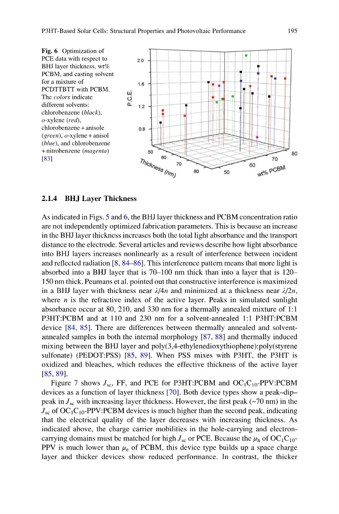
As indicated in Figs. 5 and 6, the BHJ layer thickness and PCBM concentration ratio
are not independently optimized fabrication parameters. This is because an increase
in the BHJ layer thickness increases both the total light absorbance and the transport
distance to the electrode. Several articles and reviews describe how light absorbance
into BHJ layers increases nonlinearly as a result of interference between incident
and reflected radiation [8, 84–86]. This interference pattern means that more light is
absorbed into a BHJ layer that is 70–100 nm thick than into a layer that is 120–
150 nm thick. Peumans et al. pointed out that constructive interference is maximized
in a BHJ layer with thickness near λ/4n and minimized at a thickness near λ/2n,
where n is the refractive index of the active layer. Peaks in simulated sunlight
absorbance occur at 80, 210, and 330 nm for a thermally annealed mixture of 1:1
P3HT:PCBM and at 110 and 230 nm for a solvent-annealed 1:1 P3HT:PCBM
device [84, 85]. There are differences between thermally annealed and solventannealed samples in both the internal morphology [87, 88] and thermally induced
mixing between the BHJ layer and poly(3,4-ethylenedioxythiophene):poly(styrene
sulfonate) (PEDOT:PSS) [85, 89]. When PSS mixes with P3HT, the P3HT is
oxidized and bleaches, which reduces the effective thickness of the active layer
[85, 89].
Figure 7 shows J sc , FF, and PCE for P3HT:PCBM and OC 1 C 10 -PPV:PCBM
devices as a function of layer thickness [70]. Both device types show a peak–dip–
peak in J sc with increasing layer thickness. However, the first peak (~70 nm) in the
J sc of OC 1 C 10 -PPV:PCBM devices is much higher than the second peak, indicating
that the electrical quality of the layer decreases with increasing thickness. As
indicated above, the charge carrier mobilities in the hole-carrying and electroncarrying domains must be matched for high J sc or PCE. Because the μ h of OC 1 C 10 -
PPV is much lower than μ e of PCBM, this device type builds up a space charge
layer and thicker devices show reduced performance. In contrast, the thicker
Fig. 6 Optimization of
PCE data with respect to
BHJ layer thickness, wt%
PCBM, and casting solvent
for a mixture of
PCDTTBTT with PCBM.
The colors indicate
different solvents:
chlorobenzene (black),
o-xylene (red),
chlorobenzene + anisole
(green), o-xylene + anisol
(blue), and chlorobenzene
+ nitrobenzene (magenta)
[83]
P3HT-Based Solar Cells: Structural Properties and Photovoltaic Performance
195
As indicated in Figs. 5 and 6, the BHJ layer thickness and PCBM concentration ratio
are not independently optimized fabrication parameters. This is because an increase
in the BHJ layer thickness increases both the total light absorbance and the transport
distance to the electrode. Several articles and reviews describe how light absorbance
into BHJ layers increases nonlinearly as a result of interference between incident
and reflected radiation [8, 84–86]. This interference pattern means that more light is
absorbed into a BHJ layer that is 70–100 nm thick than into a layer that is 120–
150 nm thick. Peumans et al. pointed out that constructive interference is maximized
in a BHJ layer with thickness near λ/4n and minimized at a thickness near λ/2n,
where n is the refractive index of the active layer. Peaks in simulated sunlight
absorbance occur at 80, 210, and 330 nm for a thermally annealed mixture of 1:1
P3HT:PCBM and at 110 and 230 nm for a solvent-annealed 1:1 P3HT:PCBM
device [84, 85]. There are differences between thermally annealed and solventannealed samples in both the internal morphology [87, 88] and thermally induced
mixing between the BHJ layer and poly(3,4-ethylenedioxythiophene):poly(styrene
sulfonate) (PEDOT:PSS) [85, 89]. When PSS mixes with P3HT, the P3HT is
oxidized and bleaches, which reduces the effective thickness of the active layer
[85, 89].
Figure 7 shows J sc , FF, and PCE for P3HT:PCBM and OC 1 C 10 -PPV:PCBM
devices as a function of layer thickness [70]. Both device types show a peak–dip–
peak in J sc with increasing layer thickness. However, the first peak (~70 nm) in the
J sc of OC 1 C 10 -PPV:PCBM devices is much higher than the second peak, indicating
that the electrical quality of the layer decreases with increasing thickness. As
indicated above, the charge carrier mobilities in the hole-carrying and electroncarrying domains must be matched for high J sc or PCE. Because the μ h of OC 1 C 10 -
PPV is much lower than μ e of PCBM, this device type builds up a space charge
layer and thicker devices show reduced performance. In contrast, the thicker
Fig. 6 Optimization of
PCE data with respect to
BHJ layer thickness, wt%
PCBM, and casting solvent
for a mixture of
PCDTTBTT with PCBM.
The colors indicate
different solvents:
chlorobenzene (black),
o-xylene (red),
chlorobenzene + anisole
(green), o-xylene + anisol
(blue), and chlorobenzene
+ nitrobenzene (magenta)
[83]
P3HT-Based Solar Cells: Structural Properties and Photovoltaic Performance
195