

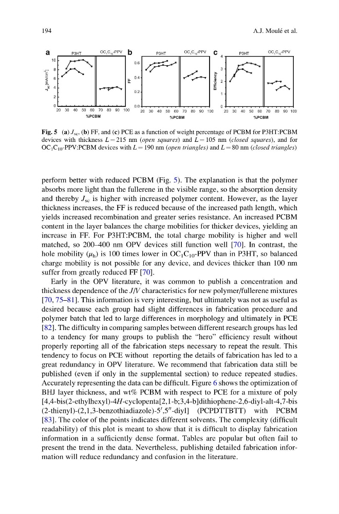
perform better with reduced PCBM (Fig. 5). The explanation is that the polymer
absorbs more light than the fullerene in the visible range, so the absorption density
and thereby J sc is higher with increased polymer content. However, as the layer
thickness increases, the FF is reduced because of the increased path length, which
yields increased recombination and greater series resistance. An increased PCBM
content in the layer balances the charge mobilities for thicker devices, yielding an
increase in FF. For P3HT:PCBM, the total charge mobility is higher and well
matched, so 200–400 nm OPV devices still function well [70]. In contrast, the
hole mobility (μ h ) is 100 times lower in OC 1 C 10 -PPV than in P3HT, so balanced
charge mobility is not possible for any device, and devices thicker than 100 nm
suffer from greatly reduced FF [70].
Early in the OPV literature, it was common to publish a concentration and
thickness dependence of the J/V characteristics for new polymer/fullerene mixtures
[70, 75–81]. This information is very interesting, but ultimately was not as useful as
desired because each group had slight differences in fabrication procedure and
polymer batch that led to large differences in morphology and ultimately in PCE
[82]. The difficulty in comparing samples between different research groups has led
to a tendency for many groups to publish the “hero” efficiency result without
properly reporting all of the fabrication steps necessary to repeat the result. This
tendency to focus on PCE without reporting the details of fabrication has led to a
great redundancy in OPV literature. We recommend that fabrication data still be
published (even if only in the supplemental section) to reduce repeated studies.
Accurately representing the data can be difficult. Figure 6 shows the optimization of
BHJ layer thickness, and wt% PCBM with respect to PCE for a mixture of poly
[4,4-bis(2-ethylhexyl)-4H-cyclopenta[2,1-b;3,4-b]dithiophene-2,6-diyl-alt-4,7-bis
(2-thienyl)-(2,1,3-benzothiadiazole)-5
0 ,5
00 -diyl] (PCPDTTBTT) with PCBM
[83]. The color of the points indicates different solvents. The complexity (difficult
readability) of this plot is meant to show that it is difficult to display fabrication
information in a sufficiently dense format. Tables are popular but often fail to
present the trend in the data. Nevertheless, publishing detailed fabrication information will reduce redundancy and confusion in the literature.
P3HT
0
2
4
6
8
10
J
SC
[mA/cm
2
]
20 30 40 50 60 70 80 90 100
0.0
0.2
0.4
0.6
FF
20 30 40 50 60 70 80 90 100
0
1
2
3
4
Efficiency
%PCBM
%PCBM
20 30 40 50 60 70 80 90 100
%PCBM
P3HT
P3HT
OC 1 C 10 -PPV
OC 1 C 10 -PPV
OC 1 C 10 -PPV
a
b
c
Fig. 5 (a) J sc , (b) FF, and (c) PCE as a function of weight percentage of PCBM for P3HT:PCBM
devices with thickness L ¼ 215 nm (open squares) and L ¼ 105 nm (closed squares), and for
OC 1 C 10 -PPV:PCBM devices with L ¼ 190 nm (open triangles) and L ¼ 80 nm (closed triangles)
194
A.J. Moule ´ et al.
absorbs more light than the fullerene in the visible range, so the absorption density
and thereby J sc is higher with increased polymer content. However, as the layer
thickness increases, the FF is reduced because of the increased path length, which
yields increased recombination and greater series resistance. An increased PCBM
content in the layer balances the charge mobilities for thicker devices, yielding an
increase in FF. For P3HT:PCBM, the total charge mobility is higher and well
matched, so 200–400 nm OPV devices still function well [70]. In contrast, the
hole mobility (μ h ) is 100 times lower in OC 1 C 10 -PPV than in P3HT, so balanced
charge mobility is not possible for any device, and devices thicker than 100 nm
suffer from greatly reduced FF [70].
Early in the OPV literature, it was common to publish a concentration and
thickness dependence of the J/V characteristics for new polymer/fullerene mixtures
[70, 75–81]. This information is very interesting, but ultimately was not as useful as
desired because each group had slight differences in fabrication procedure and
polymer batch that led to large differences in morphology and ultimately in PCE
[82]. The difficulty in comparing samples between different research groups has led
to a tendency for many groups to publish the “hero” efficiency result without
properly reporting all of the fabrication steps necessary to repeat the result. This
tendency to focus on PCE without reporting the details of fabrication has led to a
great redundancy in OPV literature. We recommend that fabrication data still be
published (even if only in the supplemental section) to reduce repeated studies.
Accurately representing the data can be difficult. Figure 6 shows the optimization of
BHJ layer thickness, and wt% PCBM with respect to PCE for a mixture of poly
[4,4-bis(2-ethylhexyl)-4H-cyclopenta[2,1-b;3,4-b]dithiophene-2,6-diyl-alt-4,7-bis
(2-thienyl)-(2,1,3-benzothiadiazole)-5
0 ,5
00 -diyl] (PCPDTTBTT) with PCBM
[83]. The color of the points indicates different solvents. The complexity (difficult
readability) of this plot is meant to show that it is difficult to display fabrication
information in a sufficiently dense format. Tables are popular but often fail to
present the trend in the data. Nevertheless, publishing detailed fabrication information will reduce redundancy and confusion in the literature.
P3HT
0
2
4
6
8
10
J
SC
[mA/cm
2
]
20 30 40 50 60 70 80 90 100
0.0
0.2
0.4
0.6
FF
20 30 40 50 60 70 80 90 100
0
1
2
3
4
Efficiency
%PCBM
%PCBM
20 30 40 50 60 70 80 90 100
%PCBM
P3HT
P3HT
OC 1 C 10 -PPV
OC 1 C 10 -PPV
OC 1 C 10 -PPV
a
b
c
Fig. 5 (a) J sc , (b) FF, and (c) PCE as a function of weight percentage of PCBM for P3HT:PCBM
devices with thickness L ¼ 215 nm (open squares) and L ¼ 105 nm (closed squares), and for
OC 1 C 10 -PPV:PCBM devices with L ¼ 190 nm (open triangles) and L ¼ 80 nm (closed triangles)
194
A.J. Moule ´ et al.