

12.4 Deposition with the Help of Tips
467
However, this method leads to unpredictable events, and potential sweeps are clearly
not possible to run up to the user’s need.
Application of tungsten nanotip for nanoelectrode fabrication is possible if the
sharp tip is covered well enough sidewise. This can be carried out by electrophoretic
painting [184]. This coating method eliminated any manual step but leaves the very
end of the W tip still electroactive for a further deposition of Au particle. The electrode
size thus achieved was above 60 nm.
Another important step in the electrochemical nanoelectrode fabrication was when
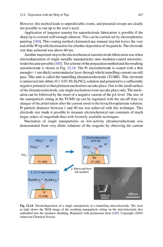
electrodeposition of single metallic nanoparticles onto insulator-coated microelectrodes became possible [185]. The scheme of the preparation method and the resulting
nanoelectrode is shown in Fig. 12.14. The Pt microelectrode is coated with a thin
enough (~1 nm thick) semiconductor layer through which tunnelling current can still
pass. This unit is called the tunnelling ultramicroelectrode (TUME). This electrode
is immersed into dilute (0.1-0.01 M) H 2 PtCl 6 solution and polarized to a sufficiently
negative potential so that platinum nucleation can take place. Due to the small surface
of the ultramicroelectrode, one single nucleation event can take place only. The nucleation can be followed by the onset of a negative current of the pA level. The size of
the nanoparticle sitting at the TUME tip can be regulated with the cut-off time (or
charge) of the polarization after the current onset in the hexachloroplatinate solution.
Pt particle diameter between 1 and 40 nm was achieved with this technique. This
electrode size made it possible to measure electrochemical rate constants of much
larger orders of magnitude than with formerly available techniques.
Nucleation of single nanoparticles on low-activity ultramicroelectrode was
demonstrated from very dilute solutions of the reagents by observing the current
Fig. 12.14 Electrodeposition of a single nanoparticle at a tunnelling microelectrode. The inset
at right shows the SEM image of the resulting nanoparticle sitting on the microelectrode disc
embedded into the insulator shielding. Reprinted with permission from [185]. Copyright (2016)
American Chemical Society
467
However, this method leads to unpredictable events, and potential sweeps are clearly
not possible to run up to the user’s need.
Application of tungsten nanotip for nanoelectrode fabrication is possible if the
sharp tip is covered well enough sidewise. This can be carried out by electrophoretic
painting [184]. This coating method eliminated any manual step but leaves the very
end of the W tip still electroactive for a further deposition of Au particle. The electrode
size thus achieved was above 60 nm.
Another important step in the electrochemical nanoelectrode fabrication was when
electrodeposition of single metallic nanoparticles onto insulator-coated microelectrodes became possible [185]. The scheme of the preparation method and the resulting
nanoelectrode is shown in Fig. 12.14. The Pt microelectrode is coated with a thin
enough (~1 nm thick) semiconductor layer through which tunnelling current can still
pass. This unit is called the tunnelling ultramicroelectrode (TUME). This electrode
is immersed into dilute (0.1-0.01 M) H 2 PtCl 6 solution and polarized to a sufficiently
negative potential so that platinum nucleation can take place. Due to the small surface
of the ultramicroelectrode, one single nucleation event can take place only. The nucleation can be followed by the onset of a negative current of the pA level. The size of
the nanoparticle sitting at the TUME tip can be regulated with the cut-off time (or
charge) of the polarization after the current onset in the hexachloroplatinate solution.
Pt particle diameter between 1 and 40 nm was achieved with this technique. This
electrode size made it possible to measure electrochemical rate constants of much
larger orders of magnitude than with formerly available techniques.
Nucleation of single nanoparticles on low-activity ultramicroelectrode was
demonstrated from very dilute solutions of the reagents by observing the current
Fig. 12.14 Electrodeposition of a single nanoparticle at a tunnelling microelectrode. The inset
at right shows the SEM image of the resulting nanoparticle sitting on the microelectrode disc
embedded into the insulator shielding. Reprinted with permission from [185]. Copyright (2016)
American Chemical Society