

430
12 Localized or Spatially Selective Electrodeposition Methods
The final step of the nanowire preparation is the removal of the thin Cu deposit
of high specific surface area grown during the high-voltage intervals. The etching
process has to be mild enough and can last for a short time only to leave the wires
intact while removing the thin layers in between.
The combined technique of alternating cell voltage with post-deposition etching
is tuneable is various ways. The thickness of the copper wires can be adjusted with
the charge passed while the deposition process in within the diffusion-limited lowvoltage regime, while the interwire distance is determined by the charge passed
during the rest of the deposition cycle. The potential limits are obviously of key
importance for setting the appropriate deposition regimes, and the surface density
of the wires finally obtained is roughly proportional with the frequency of the cell
voltage variation.
The modulated-voltage deposition technique was adapted to the deposition of
parallel cobalt nanowires, too [20]. It was shown that the set of parallel nanowires
obtained after the deposition and etching process covered the substrate uniformly at
large surface areas even in the case when the substrate was intentionally corrugated
in various ways, either with randomly aligned flat areas of with highly periodic
undulations. An excellent agreement was found between SEM observations and
magnetic force microscopic images.
12.1.3 Miscellaneous Deposits Obtained in Cryostatic
Thin-Layer Cells
The precursor deposit of a micrometre-periodicity CuO/In 2 O 3 semiconductor
heterostructure array was prepared with the freezing-based thin-layer technique [21].
The starting solution contained Cu(NO 3 ) 2 and In(NO 3 ) 3 in a concentration of a few
tens of mM, and HNO 3 was added to the solution for adjusting the pH to 3. The cell
voltage was modulated between two values, the lower and the higher one leading to
a copper-containing and an indium-containing deposit, respectively. In accord with
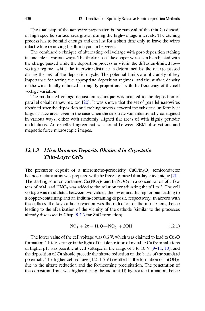
the authors, the key cathode reaction was the reduction of the nitrate ions, hence
leading to the alkalization of the vicinity of the cathode (similar to the processes
already discussed in Chap. 8.2.3 for ZnO formation):
NO
−
3 + 2e + H 2 ONO
−
2 + 2OH
−
(12.1)
The lower value of the cell voltage was 0.6 V, which was claimed to lead to Cu 2 O
formation. This is strange in the light of that deposition of metallic Cu from solutions
of higher pH was possible at cell voltages in the range of 3 to 10 V [9–11, 13], and
the deposition of Cu should precede the nitrate reduction on the basis of the standard
potentials. The higher cell voltage (1.2–1.5 V) resulted in the formation of In(OH) 3
due to the nitrate reduction and the forthcoming precipitation. The penetration of
the deposition front was higher during the indium(III) hydroxide formation, hence
12 Localized or Spatially Selective Electrodeposition Methods
The final step of the nanowire preparation is the removal of the thin Cu deposit
of high specific surface area grown during the high-voltage intervals. The etching
process has to be mild enough and can last for a short time only to leave the wires
intact while removing the thin layers in between.
The combined technique of alternating cell voltage with post-deposition etching
is tuneable is various ways. The thickness of the copper wires can be adjusted with
the charge passed while the deposition process in within the diffusion-limited lowvoltage regime, while the interwire distance is determined by the charge passed
during the rest of the deposition cycle. The potential limits are obviously of key
importance for setting the appropriate deposition regimes, and the surface density
of the wires finally obtained is roughly proportional with the frequency of the cell
voltage variation.
The modulated-voltage deposition technique was adapted to the deposition of
parallel cobalt nanowires, too [20]. It was shown that the set of parallel nanowires
obtained after the deposition and etching process covered the substrate uniformly at
large surface areas even in the case when the substrate was intentionally corrugated
in various ways, either with randomly aligned flat areas of with highly periodic
undulations. An excellent agreement was found between SEM observations and
magnetic force microscopic images.
12.1.3 Miscellaneous Deposits Obtained in Cryostatic
Thin-Layer Cells
The precursor deposit of a micrometre-periodicity CuO/In 2 O 3 semiconductor
heterostructure array was prepared with the freezing-based thin-layer technique [21].
The starting solution contained Cu(NO 3 ) 2 and In(NO 3 ) 3 in a concentration of a few
tens of mM, and HNO 3 was added to the solution for adjusting the pH to 3. The cell
voltage was modulated between two values, the lower and the higher one leading to
a copper-containing and an indium-containing deposit, respectively. In accord with
the authors, the key cathode reaction was the reduction of the nitrate ions, hence
leading to the alkalization of the vicinity of the cathode (similar to the processes
already discussed in Chap. 8.2.3 for ZnO formation):
NO
−
3 + 2e + H 2 ONO
−
2 + 2OH
−
(12.1)
The lower value of the cell voltage was 0.6 V, which was claimed to lead to Cu 2 O
formation. This is strange in the light of that deposition of metallic Cu from solutions
of higher pH was possible at cell voltages in the range of 3 to 10 V [9–11, 13], and
the deposition of Cu should precede the nitrate reduction on the basis of the standard
potentials. The higher cell voltage (1.2–1.5 V) resulted in the formation of In(OH) 3
due to the nitrate reduction and the forthcoming precipitation. The penetration of
the deposition front was higher during the indium(III) hydroxide formation, hence