

12.1 Electrodeposition in Ultrathin Solution Layers Along the Edge of the Cell
431
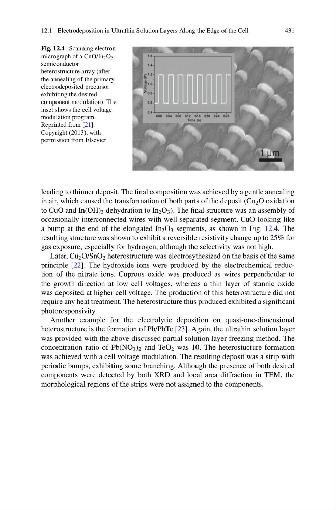
Fig. 12.4 Scanning electron
micrograph of a CuO/In 2 O 3
semiconductor
heterostructure array (after
the annealing of the primary
electrodeposited precursor
exhibiting the desired
component modulation). The
inset shows the cell voltage
modulation program.
Reprinted from [21].
Copyright (2013), with
permission from Elsevier
leading to thinner deposit. The final composition was achieved by a gentle annealing
in air, which caused the transformation of both parts of the deposit (Cu 2 O oxidation
to CuO and In(OH) 3 dehydration to In 2 O 3 ). The final structure was an assembly of
occasionally interconnected wires with well-separated segment, CuO looking like
a bump at the end of the elongated In 2 O 3 segments, as shown in Fig. 12.4. The
resulting structure was shown to exhibit a reversible resistivity change up to 25% for
gas exposure, especially for hydrogen, although the selectivity was not high.
Later, Cu 2 O/SnO 2 heterostructure was electrosythesized on the basis of the same
principle [22]. The hydroxide ions were produced by the electrochemical reduction of the nitrate ions. Cuprous oxide was produced as wires perpendicular to
the growth direction at low cell voltages, whereas a thin layer of stannic oxide
was deposited at higher cell voltage. The production of this heterostructure did not
require any heat treatment. The heterostructure thus produced exhibited a significant
photoresponsivity.
Another example for the electrolytic deposition on quasi-one-dimensional
heterostructure is the formation of Pb/PbTe [23]. Again, the ultrathin solution layer
was provided with the above-discussed partial solution layer freezing method. The
concentration ratio of Pb(NO 3 ) 2 and TeO 2 was 10. The heterostucture formation
was achieved with a cell voltage modulation. The resulting deposit was a strip with
periodic bumps, exhibiting some branching. Although the presence of both desired
components were detected by both XRD and local area diffraction in TEM, the
morphological regions of the strips were not assigned to the components.
431
Fig. 12.4 Scanning electron
micrograph of a CuO/In 2 O 3
semiconductor
heterostructure array (after
the annealing of the primary
electrodeposited precursor
exhibiting the desired
component modulation). The
inset shows the cell voltage
modulation program.
Reprinted from [21].
Copyright (2013), with
permission from Elsevier
leading to thinner deposit. The final composition was achieved by a gentle annealing
in air, which caused the transformation of both parts of the deposit (Cu 2 O oxidation
to CuO and In(OH) 3 dehydration to In 2 O 3 ). The final structure was an assembly of
occasionally interconnected wires with well-separated segment, CuO looking like
a bump at the end of the elongated In 2 O 3 segments, as shown in Fig. 12.4. The
resulting structure was shown to exhibit a reversible resistivity change up to 25% for
gas exposure, especially for hydrogen, although the selectivity was not high.
Later, Cu 2 O/SnO 2 heterostructure was electrosythesized on the basis of the same
principle [22]. The hydroxide ions were produced by the electrochemical reduction of the nitrate ions. Cuprous oxide was produced as wires perpendicular to
the growth direction at low cell voltages, whereas a thin layer of stannic oxide
was deposited at higher cell voltage. The production of this heterostructure did not
require any heat treatment. The heterostructure thus produced exhibited a significant
photoresponsivity.
Another example for the electrolytic deposition on quasi-one-dimensional
heterostructure is the formation of Pb/PbTe [23]. Again, the ultrathin solution layer
was provided with the above-discussed partial solution layer freezing method. The
concentration ratio of Pb(NO 3 ) 2 and TeO 2 was 10. The heterostucture formation
was achieved with a cell voltage modulation. The resulting deposit was a strip with
periodic bumps, exhibiting some branching. Although the presence of both desired
components were detected by both XRD and local area diffraction in TEM, the
morphological regions of the strips were not assigned to the components.