

12.1 Electrodeposition in Ultrathin Solution Layers Along the Edge of the Cell
429
It was speculated that the formation of ZnO is related to the oxygen content of the
solution. However, the commonality of the oscillation pattern with the Cu deposition
system indicates that a common reason may stand behind the oscillatory behaviour
that is related to the lack of the supporting electrolyte, to the hydrolysis of the cations,
to the deposition rate beyond the diffusion-limited regime and to the high negative
potential of the cathode.
Finally, it is to be mentioned that the chilled thin-layer cell technique with the
combination of a post-deposition etching step was adapted for copper nanowire
deposition on non-patterned silicon surface [19]. Here, the cell voltage was modulated
during the deposition. The authors chose a semi-sine waveform for the cell voltage.
The pronounced opinion of the author of this book is, however, that the waveform is
of little importance if the extremes of the cell voltage comprise the desired deposition
regimes at the cathode. Namely, at small cell voltage copper deposition takes place
with the formation of dense copper, and it is believed that the copper deposition
rate is below the diffusion-limited one. The visual observation during the growth
process confirmed that the low cell voltage is what results in the deposition of dense
but relatively thick copper. When the cell voltage is high, the advancement rate
of the growth front increases, which corresponds to the formation of a network of
tiny copper filaments (called membrane in the original work [19]). In this growth
regime, the impact of the electric field becomes important, and the resulting spongy
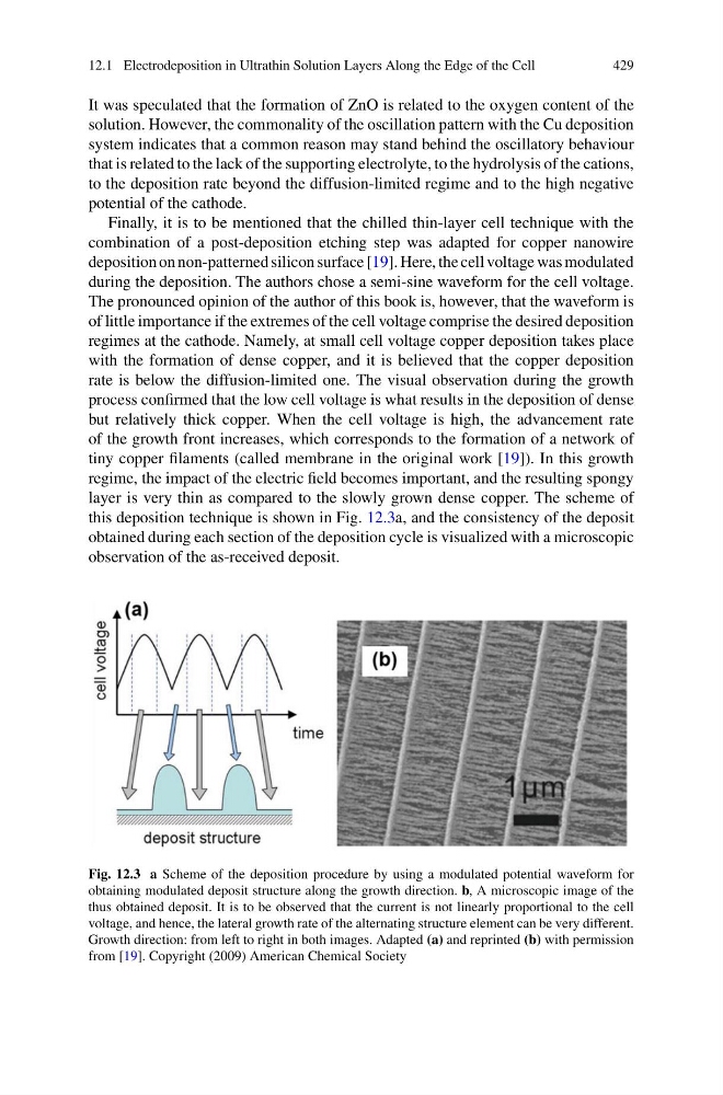
layer is very thin as compared to the slowly grown dense copper. The scheme of
this deposition technique is shown in Fig. 12.3a, and the consistency of the deposit
obtained during each section of the deposition cycle is visualized with a microscopic
observation of the as-received deposit.
Fig. 12.3 a Scheme of the deposition procedure by using a modulated potential waveform for
obtaining modulated deposit structure along the growth direction. b, A microscopic image of the
thus obtained deposit. It is to be observed that the current is not linearly proportional to the cell
voltage, and hence, the lateral growth rate of the alternating structure element can be very different.
Growth direction: from left to right in both images. Adapted (a) and reprinted (b) with permission
from [19]. Copyright (2009) American Chemical Society
429
It was speculated that the formation of ZnO is related to the oxygen content of the
solution. However, the commonality of the oscillation pattern with the Cu deposition
system indicates that a common reason may stand behind the oscillatory behaviour
that is related to the lack of the supporting electrolyte, to the hydrolysis of the cations,
to the deposition rate beyond the diffusion-limited regime and to the high negative
potential of the cathode.
Finally, it is to be mentioned that the chilled thin-layer cell technique with the
combination of a post-deposition etching step was adapted for copper nanowire
deposition on non-patterned silicon surface [19]. Here, the cell voltage was modulated
during the deposition. The authors chose a semi-sine waveform for the cell voltage.
The pronounced opinion of the author of this book is, however, that the waveform is
of little importance if the extremes of the cell voltage comprise the desired deposition
regimes at the cathode. Namely, at small cell voltage copper deposition takes place
with the formation of dense copper, and it is believed that the copper deposition
rate is below the diffusion-limited one. The visual observation during the growth
process confirmed that the low cell voltage is what results in the deposition of dense
but relatively thick copper. When the cell voltage is high, the advancement rate
of the growth front increases, which corresponds to the formation of a network of
tiny copper filaments (called membrane in the original work [19]). In this growth
regime, the impact of the electric field becomes important, and the resulting spongy
layer is very thin as compared to the slowly grown dense copper. The scheme of
this deposition technique is shown in Fig. 12.3a, and the consistency of the deposit
obtained during each section of the deposition cycle is visualized with a microscopic
observation of the as-received deposit.
Fig. 12.3 a Scheme of the deposition procedure by using a modulated potential waveform for
obtaining modulated deposit structure along the growth direction. b, A microscopic image of the
thus obtained deposit. It is to be observed that the current is not linearly proportional to the cell
voltage, and hence, the lateral growth rate of the alternating structure element can be very different.
Growth direction: from left to right in both images. Adapted (a) and reprinted (b) with permission
from [19]. Copyright (2009) American Chemical Society