

10.4 Electrodeposition on Surfaces with Mechanically …
339
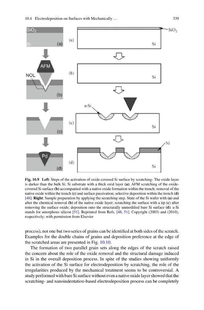
Fig. 10.9 Left: Steps of the activation of oxide-covered Si surface by scratching- The oxide layer
is darker than the bulk Si. Si substrate with a thick oxid layer (a); AFM scratching of the oxidecovered Si surface (b) accompanied with a native oxide formation within the trench; removal of the
native oxide within the trench (c) and surface passivation; selective deposition within the trench (d)
[48]. Right: Sample preparation by applying the scratching step. State of the Si wafer with (a) and
after the chemical removal (b) of the native oxide layer; scratching the surface with a tip (c) after
removing the surface oxide; deposition onto the structurally unmodified bare Si surface (d). a-Si
stands for amorphous silicon [51]. Reprinted from Refs. [48, 51]. Copyright (2003) and (2010),
respectively; with permission from Elsevier
process), not one but two series of grains can be identified at both sides of the scratch.
Examples for the double chains of grains and deposition preference at the edge of
the scratched areas are presented in Fig. 10.10.
The formation of two parallel grain sets along the edges of the scratch raised
the concern about the role of the oxide removal and the structural damage induced
in Si in the overall deposition process. In spite of the studies showing uniformly
the activation of the Si surface for electrodeposition by scratching, the role of the
irregularities produced by the mechanical treatment seems to be controversial. A
study performed with bare Si surface without even a native oxide layer showed that the
scratching- and nanoindentation-based electrodeposition process can be completely
339
Fig. 10.9 Left: Steps of the activation of oxide-covered Si surface by scratching- The oxide layer
is darker than the bulk Si. Si substrate with a thick oxid layer (a); AFM scratching of the oxidecovered Si surface (b) accompanied with a native oxide formation within the trench; removal of the
native oxide within the trench (c) and surface passivation; selective deposition within the trench (d)
[48]. Right: Sample preparation by applying the scratching step. State of the Si wafer with (a) and
after the chemical removal (b) of the native oxide layer; scratching the surface with a tip (c) after
removing the surface oxide; deposition onto the structurally unmodified bare Si surface (d). a-Si
stands for amorphous silicon [51]. Reprinted from Refs. [48, 51]. Copyright (2003) and (2010),
respectively; with permission from Elsevier
process), not one but two series of grains can be identified at both sides of the scratch.
Examples for the double chains of grains and deposition preference at the edge of
the scratched areas are presented in Fig. 10.10.
The formation of two parallel grain sets along the edges of the scratch raised
the concern about the role of the oxide removal and the structural damage induced
in Si in the overall deposition process. In spite of the studies showing uniformly
the activation of the Si surface for electrodeposition by scratching, the role of the
irregularities produced by the mechanical treatment seems to be controversial. A
study performed with bare Si surface without even a native oxide layer showed that the
scratching- and nanoindentation-based electrodeposition process can be completely