

340
10 Electrochemical Manufacturing Methods Based on Surface …
a
c
b
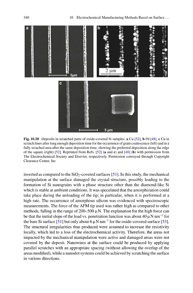
Fig. 10.10 Deposits in scratched parts of oxide-covered Si samples. a Cu [52], b Pd [48], c Cu in
scratch lines after long enough deposition time for the occurrence of grain coalescence (left) and in a
fully scrached area after the same deposition time, showing the preferred deposition along the edge
of the square (right) [52]. Reprinted from Refs. [52] (a and c) and [48] (b) with permission from
The Electrochemical Society and Elsevier, respectively. Permission conveyed through Copyright
Clearance Center, Inc
inverted as compared to the SiO 2 -covered surfaces [51]. In this study, the mechanical
manipulation at the surface damaged the crystal structure, possibly leading to the
formation of Si nanograins with a phase structure other than the diamond-like Si
which is stable at ambient conditions. It was speculated that the amorphization could
take place during the unloading of the tip; in particular, when it is performed at a
high rate. The occurrence of amorphous silicon was evidenced with spectroscopic
measurements. The force of the AFM tip used was rather high as compared to other
methods, falling in the range of 200–500 μN. The explanation for the high force can
be that the initial slope of the load vs. penetration function was about 40 μN nm
–1 for
the bare Si surface [51] but only about 6 μN nm
–1 for the oxide-covered surface [53].
The structural irregularities thus produced were assumed to increase the resistivity
locally, which led to a loss of the electrochemical activity. Therefore, the areas not
impacted by the mechanical manipulation were active and damaged areas were not
covered by the deposit. Nanowires at the surface could be produced by applying
parallel scratches with an appropriate spacing (without allowing the overlap of the
areas modified), while a nanodot systems could be achieved by scratching the surface
in various directions.
10 Electrochemical Manufacturing Methods Based on Surface …
a
c
b
Fig. 10.10 Deposits in scratched parts of oxide-covered Si samples. a Cu [52], b Pd [48], c Cu in
scratch lines after long enough deposition time for the occurrence of grain coalescence (left) and in a
fully scrached area after the same deposition time, showing the preferred deposition along the edge
of the square (right) [52]. Reprinted from Refs. [52] (a and c) and [48] (b) with permission from
The Electrochemical Society and Elsevier, respectively. Permission conveyed through Copyright
Clearance Center, Inc
inverted as compared to the SiO 2 -covered surfaces [51]. In this study, the mechanical
manipulation at the surface damaged the crystal structure, possibly leading to the
formation of Si nanograins with a phase structure other than the diamond-like Si
which is stable at ambient conditions. It was speculated that the amorphization could
take place during the unloading of the tip; in particular, when it is performed at a
high rate. The occurrence of amorphous silicon was evidenced with spectroscopic
measurements. The force of the AFM tip used was rather high as compared to other
methods, falling in the range of 200–500 μN. The explanation for the high force can
be that the initial slope of the load vs. penetration function was about 40 μN nm
–1 for
the bare Si surface [51] but only about 6 μN nm
–1 for the oxide-covered surface [53].
The structural irregularities thus produced were assumed to increase the resistivity
locally, which led to a loss of the electrochemical activity. Therefore, the areas not
impacted by the mechanical manipulation were active and damaged areas were not
covered by the deposit. Nanowires at the surface could be produced by applying
parallel scratches with an appropriate spacing (without allowing the overlap of the
areas modified), while a nanodot systems could be achieved by scratching the surface
in various directions.