

338
10 Electrochemical Manufacturing Methods Based on Surface …
a
b
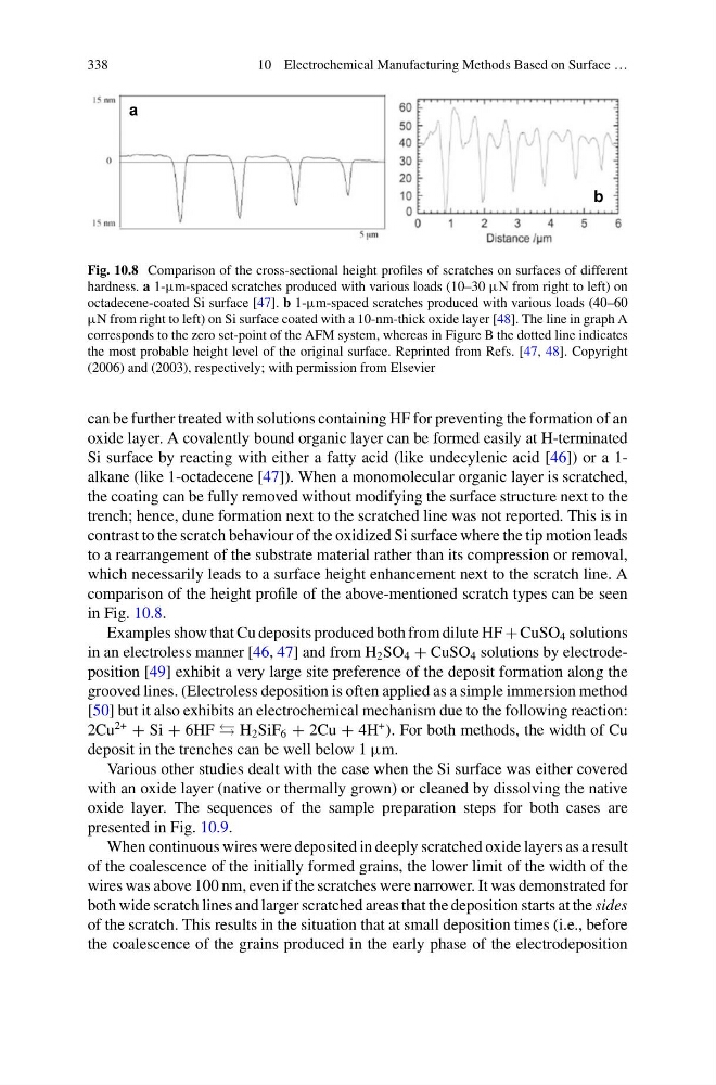
Fig. 10.8 Comparison of the cross-sectional height profiles of scratches on surfaces of different
hardness. a 1-μm-spaced scratches produced with various loads (10–30 μN from right to left) on
octadecene-coated Si surface [47]. b 1-μm-spaced scratches produced with various loads (40–60
μN from right to left) on Si surface coated with a 10-nm-thick oxide layer [48]. The line in graph A
corresponds to the zero set-point of the AFM system, whereas in Figure B the dotted line indicates
the most probable height level of the original surface. Reprinted from Refs. [47, 48]. Copyright
(2006) and (2003), respectively; with permission from Elsevier
can be further treated with solutions containing HF for preventing the formation of an
oxide layer. A covalently bound organic layer can be formed easily at H-terminated
Si surface by reacting with either a fatty acid (like undecylenic acid [46]) or a 1alkane (like 1-octadecene [47]). When a monomolecular organic layer is scratched,
the coating can be fully removed without modifying the surface structure next to the
trench; hence, dune formation next to the scratched line was not reported. This is in
contrast to the scratch behaviour of the oxidized Si surface where the tip motion leads
to a rearrangement of the substrate material rather than its compression or removal,
which necessarily leads to a surface height enhancement next to the scratch line. A
comparison of the height profile of the above-mentioned scratch types can be seen
in Fig. 10.8.
Examples show that Cu deposits produced both from dilute HF + CuSO 4 solutions
in an electroless manner [46, 47] and from H 2 SO 4 + CuSO 4 solutions by electrodeposition [49] exhibit a very large site preference of the deposit formation along the
grooved lines. (Electroless deposition is often applied as a simple immersion method
[50] but it also exhibits an electrochemical mechanism due to the following reaction:
2Cu
2+
+ Si + 6HF H 2 SiF 6 + 2Cu + 4H
+ ). For both methods, the width of Cu
deposit in the trenches can be well below 1 μm.
Various other studies dealt with the case when the Si surface was either covered
with an oxide layer (native or thermally grown) or cleaned by dissolving the native
oxide layer. The sequences of the sample preparation steps for both cases are
presented in Fig. 10.9.
When continuous wires were deposited in deeply scratched oxide layers as a result
of the coalescence of the initially formed grains, the lower limit of the width of the
wires was above 100 nm, even if the scratches were narrower. It was demonstrated for
both wide scratch lines and larger scratched areas that the deposition starts at the sides
of the scratch. This results in the situation that at small deposition times (i.e., before
the coalescence of the grains produced in the early phase of the electrodeposition
10 Electrochemical Manufacturing Methods Based on Surface …
a
b
Fig. 10.8 Comparison of the cross-sectional height profiles of scratches on surfaces of different
hardness. a 1-μm-spaced scratches produced with various loads (10–30 μN from right to left) on
octadecene-coated Si surface [47]. b 1-μm-spaced scratches produced with various loads (40–60
μN from right to left) on Si surface coated with a 10-nm-thick oxide layer [48]. The line in graph A
corresponds to the zero set-point of the AFM system, whereas in Figure B the dotted line indicates
the most probable height level of the original surface. Reprinted from Refs. [47, 48]. Copyright
(2006) and (2003), respectively; with permission from Elsevier
can be further treated with solutions containing HF for preventing the formation of an
oxide layer. A covalently bound organic layer can be formed easily at H-terminated
Si surface by reacting with either a fatty acid (like undecylenic acid [46]) or a 1alkane (like 1-octadecene [47]). When a monomolecular organic layer is scratched,
the coating can be fully removed without modifying the surface structure next to the
trench; hence, dune formation next to the scratched line was not reported. This is in
contrast to the scratch behaviour of the oxidized Si surface where the tip motion leads
to a rearrangement of the substrate material rather than its compression or removal,
which necessarily leads to a surface height enhancement next to the scratch line. A
comparison of the height profile of the above-mentioned scratch types can be seen
in Fig. 10.8.
Examples show that Cu deposits produced both from dilute HF + CuSO 4 solutions
in an electroless manner [46, 47] and from H 2 SO 4 + CuSO 4 solutions by electrodeposition [49] exhibit a very large site preference of the deposit formation along the
grooved lines. (Electroless deposition is often applied as a simple immersion method
[50] but it also exhibits an electrochemical mechanism due to the following reaction:
2Cu
2+
+ Si + 6HF H 2 SiF 6 + 2Cu + 4H
+ ). For both methods, the width of Cu
deposit in the trenches can be well below 1 μm.
Various other studies dealt with the case when the Si surface was either covered
with an oxide layer (native or thermally grown) or cleaned by dissolving the native
oxide layer. The sequences of the sample preparation steps for both cases are
presented in Fig. 10.9.
When continuous wires were deposited in deeply scratched oxide layers as a result
of the coalescence of the initially formed grains, the lower limit of the width of the
wires was above 100 nm, even if the scratches were narrower. It was demonstrated for
both wide scratch lines and larger scratched areas that the deposition starts at the sides
of the scratch. This results in the situation that at small deposition times (i.e., before
the coalescence of the grains produced in the early phase of the electrodeposition