

5.4 Properties of Electrodeposited CMAs
161
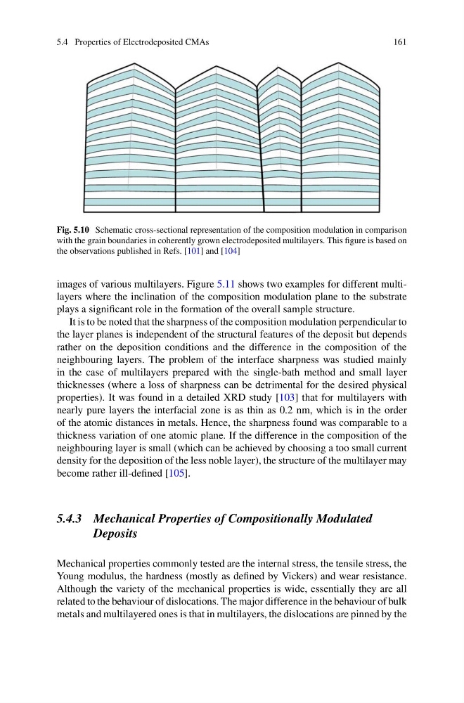
Fig. 5.10 Schematic cross-sectional representation of the composition modulation in comparison
with the grain boundaries in coherently grown electrodeposited multilayers. This figure is based on
the observations published in Refs. [101] and [104]
images of various multilayers. Figure 5.11 shows two examples for different multilayers where the inclination of the composition modulation plane to the substrate
plays a significant role in the formation of the overall sample structure.
It is to be noted that the sharpness of the composition modulation perpendicular to
the layer planes is independent of the structural features of the deposit but depends
rather on the deposition conditions and the difference in the composition of the
neighbouring layers. The problem of the interface sharpness was studied mainly
in the case of multilayers prepared with the single-bath method and small layer
thicknesses (where a loss of sharpness can be detrimental for the desired physical
properties). It was found in a detailed XRD study [103] that for multilayers with
nearly pure layers the interfacial zone is as thin as 0.2 nm, which is in the order
of the atomic distances in metals. Hence, the sharpness found was comparable to a
thickness variation of one atomic plane. If the difference in the composition of the
neighbouring layer is small (which can be achieved by choosing a too small current
density for the deposition of the less noble layer), the structure of the multilayer may
become rather ill-defined [105].
5.4.3 Mechanical Properties of Compositionally Modulated
Deposits
Mechanical properties commonly tested are the internal stress, the tensile stress, the
Young modulus, the hardness (mostly as defined by Vickers) and wear resistance.
Although the variety of the mechanical properties is wide, essentially they are all
related to the behaviour of dislocations. The major difference in the behaviour of bulk
metals and multilayered ones is that in multilayers, the dislocations are pinned by the
161
Fig. 5.10 Schematic cross-sectional representation of the composition modulation in comparison
with the grain boundaries in coherently grown electrodeposited multilayers. This figure is based on
the observations published in Refs. [101] and [104]
images of various multilayers. Figure 5.11 shows two examples for different multilayers where the inclination of the composition modulation plane to the substrate
plays a significant role in the formation of the overall sample structure.
It is to be noted that the sharpness of the composition modulation perpendicular to
the layer planes is independent of the structural features of the deposit but depends
rather on the deposition conditions and the difference in the composition of the
neighbouring layers. The problem of the interface sharpness was studied mainly
in the case of multilayers prepared with the single-bath method and small layer
thicknesses (where a loss of sharpness can be detrimental for the desired physical
properties). It was found in a detailed XRD study [103] that for multilayers with
nearly pure layers the interfacial zone is as thin as 0.2 nm, which is in the order
of the atomic distances in metals. Hence, the sharpness found was comparable to a
thickness variation of one atomic plane. If the difference in the composition of the
neighbouring layer is small (which can be achieved by choosing a too small current
density for the deposition of the less noble layer), the structure of the multilayer may
become rather ill-defined [105].
5.4.3 Mechanical Properties of Compositionally Modulated
Deposits
Mechanical properties commonly tested are the internal stress, the tensile stress, the
Young modulus, the hardness (mostly as defined by Vickers) and wear resistance.
Although the variety of the mechanical properties is wide, essentially they are all
related to the behaviour of dislocations. The major difference in the behaviour of bulk
metals and multilayered ones is that in multilayers, the dislocations are pinned by the