

2.1 Definition of the Work Function
9
metal
semiconductor
Insulator
energy
Band
gap
Conducon
band
Fermi
level
vacuum
level
work
func
IE
EA
Conducon
band
Valence
band
Valence
band
IE
EA
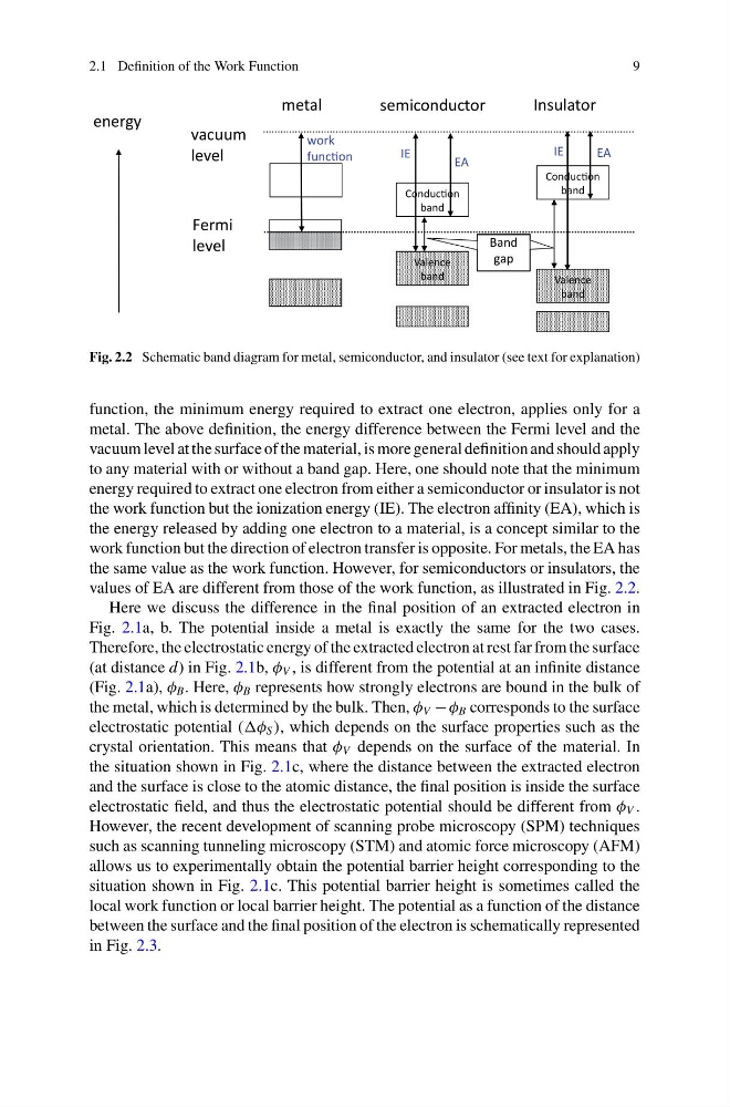
Fig. 2.2 Schematic band diagram for metal, semiconductor, and insulator (see text for explanation)
function, the minimum energy required to extract one electron, applies only for a
metal. The above definition, the energy difference between the Fermi level and the
vacuum level at the surface of the material, is more general definition and should apply
to any material with or without a band gap. Here, one should note that the minimum
energy required to extract one electron from either a semiconductor or insulator is not
the work function but the ionization energy (IE). The electron affinity (EA), which is
the energy released by adding one electron to a material, is a concept similar to the
work function but the direction of electron transfer is opposite. For metals, the EA has
the same value as the work function. However, for semiconductors or insulators, the
values of EA are different from those of the work function, as illustrated in Fig. 2.2.
Here we discuss the difference in the final position of an extracted electron in
Fig. 2.1a, b. The potential inside a metal is exactly the same for the two cases.
Therefore, the electrostatic energy of the extracted electron at rest far from the surface
(at distance d) in Fig. 2.1b, φ V , is different from the potential at an infinite distance
(Fig. 2.1a), φ B . Here, φ B represents how strongly electrons are bound in the bulk of
the metal, which is determined by the bulk. Then, φ V − φ B corresponds to the surface
electrostatic potential ((φ S ), which depends on the surface properties such as the
crystal orientation. This means that φ V depends on the surface of the material. In
the situation shown in Fig. 2.1c, where the distance between the extracted electron
and the surface is close to the atomic distance, the final position is inside the surface
electrostatic field, and thus the electrostatic potential should be different from φ V .
However, the recent development of scanning probe microscopy (SPM) techniques
such as scanning tunneling microscopy (STM) and atomic force microscopy (AFM)
allows us to experimentally obtain the potential barrier height corresponding to the
situation shown in Fig. 2.1c. This potential barrier height is sometimes called the
local work function or local barrier height. The potential as a function of the distance
between the surface and the final position of the electron is schematically represented
in Fig. 2.3.
9
metal
semiconductor
Insulator
energy
Band
gap
Conducon
band
Fermi
level
vacuum
level
work
func
IE
EA
Conducon
band
Valence
band
Valence
band
IE
EA
Fig. 2.2 Schematic band diagram for metal, semiconductor, and insulator (see text for explanation)
function, the minimum energy required to extract one electron, applies only for a
metal. The above definition, the energy difference between the Fermi level and the
vacuum level at the surface of the material, is more general definition and should apply
to any material with or without a band gap. Here, one should note that the minimum
energy required to extract one electron from either a semiconductor or insulator is not
the work function but the ionization energy (IE). The electron affinity (EA), which is
the energy released by adding one electron to a material, is a concept similar to the
work function but the direction of electron transfer is opposite. For metals, the EA has
the same value as the work function. However, for semiconductors or insulators, the
values of EA are different from those of the work function, as illustrated in Fig. 2.2.
Here we discuss the difference in the final position of an extracted electron in
Fig. 2.1a, b. The potential inside a metal is exactly the same for the two cases.
Therefore, the electrostatic energy of the extracted electron at rest far from the surface
(at distance d) in Fig. 2.1b, φ V , is different from the potential at an infinite distance
(Fig. 2.1a), φ B . Here, φ B represents how strongly electrons are bound in the bulk of
the metal, which is determined by the bulk. Then, φ V − φ B corresponds to the surface
electrostatic potential ((φ S ), which depends on the surface properties such as the
crystal orientation. This means that φ V depends on the surface of the material. In
the situation shown in Fig. 2.1c, where the distance between the extracted electron
and the surface is close to the atomic distance, the final position is inside the surface
electrostatic field, and thus the electrostatic potential should be different from φ V .
However, the recent development of scanning probe microscopy (SPM) techniques
such as scanning tunneling microscopy (STM) and atomic force microscopy (AFM)
allows us to experimentally obtain the potential barrier height corresponding to the
situation shown in Fig. 2.1c. This potential barrier height is sometimes called the
local work function or local barrier height. The potential as a function of the distance
between the surface and the final position of the electron is schematically represented
in Fig. 2.3.