

134
7 Utilization of Interface Potential
Table 7.1 Drive voltages necessary to obtain a current density of 100 mA/cm 2 in EL device with
different electrodes [14] (see text for explanation)
Al LiF (0.5 nm)/Al MgO (0.5 nm)/Al
Drive voltage needed for 100 A/cm 2 current density 17 10
11
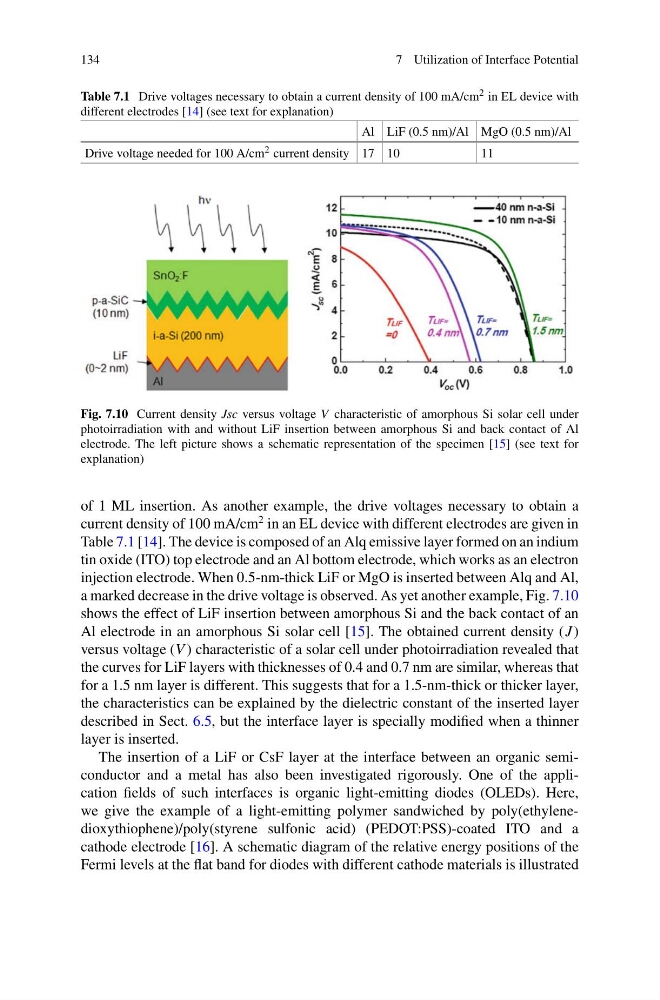
Fig. 7.10 Current density Jsc versus voltage V characteristic of amorphous Si solar cell under
photoirradiation with and without LiF insertion between amorphous Si and back contact of Al
electrode. The left picture shows a schematic representation of the specimen [15] (see text for
explanation)
of 1 ML insertion. As another example, the drive voltages necessary to obtain a
current density of 100 mA/cm
2 in an EL device with different electrodes are given in
Table 7.1 [14]. The device is composed of an Alq emissive layer formed on an indium
tin oxide (ITO) top electrode and an Al bottom electrode, which works as an electron
injection electrode. When 0.5-nm-thick LiF or MgO is inserted between Alq and Al,
a marked decrease in the drive voltage is observed. As yet another example, Fig. 7.10
shows the effect of LiF insertion between amorphous Si and the back contact of an
Al electrode in an amorphous Si solar cell [15]. The obtained current density (J )
versus voltage (V ) characteristic of a solar cell under photoirradiation revealed that
the curves for LiF layers with thicknesses of 0.4 and 0.7 nm are similar, whereas that
for a 1.5 nm layer is different. This suggests that for a 1.5-nm-thick or thicker layer,
the characteristics can be explained by the dielectric constant of the inserted layer
described in Sect. 6.5, but the interface layer is specially modified when a thinner
layer is inserted.
The insertion of a LiF or CsF layer at the interface between an organic semiconductor and a metal has also been investigated rigorously. One of the application fields of such interfaces is organic light-emitting diodes (OLEDs). Here,
we give the example of a light-emitting polymer sandwiched by poly(ethylenedioxythiophene)/poly(styrene sulfonic acid) (PEDOT:PSS)-coated ITO and a
cathode electrode [16]. A schematic diagram of the relative energy positions of the
Fermi levels at the flat band for diodes with different cathode materials is illustrated
7 Utilization of Interface Potential
Table 7.1 Drive voltages necessary to obtain a current density of 100 mA/cm 2 in EL device with
different electrodes [14] (see text for explanation)
Al LiF (0.5 nm)/Al MgO (0.5 nm)/Al
Drive voltage needed for 100 A/cm 2 current density 17 10
11
Fig. 7.10 Current density Jsc versus voltage V characteristic of amorphous Si solar cell under
photoirradiation with and without LiF insertion between amorphous Si and back contact of Al
electrode. The left picture shows a schematic representation of the specimen [15] (see text for
explanation)
of 1 ML insertion. As another example, the drive voltages necessary to obtain a
current density of 100 mA/cm
2 in an EL device with different electrodes are given in
Table 7.1 [14]. The device is composed of an Alq emissive layer formed on an indium
tin oxide (ITO) top electrode and an Al bottom electrode, which works as an electron
injection electrode. When 0.5-nm-thick LiF or MgO is inserted between Alq and Al,
a marked decrease in the drive voltage is observed. As yet another example, Fig. 7.10
shows the effect of LiF insertion between amorphous Si and the back contact of an
Al electrode in an amorphous Si solar cell [15]. The obtained current density (J )
versus voltage (V ) characteristic of a solar cell under photoirradiation revealed that
the curves for LiF layers with thicknesses of 0.4 and 0.7 nm are similar, whereas that
for a 1.5 nm layer is different. This suggests that for a 1.5-nm-thick or thicker layer,
the characteristics can be explained by the dielectric constant of the inserted layer
described in Sect. 6.5, but the interface layer is specially modified when a thinner
layer is inserted.
The insertion of a LiF or CsF layer at the interface between an organic semiconductor and a metal has also been investigated rigorously. One of the application fields of such interfaces is organic light-emitting diodes (OLEDs). Here,
we give the example of a light-emitting polymer sandwiched by poly(ethylenedioxythiophene)/poly(styrene sulfonic acid) (PEDOT:PSS)-coated ITO and a
cathode electrode [16]. A schematic diagram of the relative energy positions of the
Fermi levels at the flat band for diodes with different cathode materials is illustrated