

6.5 Generalized CNL
125
E F
metal
Semiconductor/
insulator
t m-CB
t m-VB
CB
VB
Munocc
Mocc
0
100 %
VB-derived
CB-derived
50%
ProporƟon of
orbitals forming
MIGS
CNL
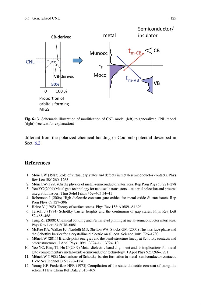
Fig. 6.13 Schematic illustration of modification of CNL model (left) to generalized CNL model
(right) (see text for explanation)
different from the polarized chemical bonding or Coulomb potential described in
Sect. 6.2.
References
1. Mönch W (1987) Role of virtual gap states and defects in metal-semiconductor contacts. Phys
Rev Lett 58:1260–1263
2. Mönch W (1990) On the physics of metal-semiconductor interfaces. Rep Prog Phys 53:221–278
3. Yeo YC (2004) Metal gate technology for nanoscale transistors—material selection and process
integration issues. Thin Solid Films 462–463:34–41
4. Robertson J (2006) High dielectric constant gate oxides for metal oxide Si transistors. Rep
Prog Phys 69:327–396
5. Heine V (1965) Theory of surface states. Phys Rev 138:A1689–A1696
6. Tersoff J (1984) Schottky barrier heights and the continuum of gap states. Phys Rev Lett
52:465–468
7. Tung RT (2000) Chemical bonding and Fermi level pinning at metal-semiconductor interfaces.
Phys Rev Lett 84:6078–6081
8. McKee RA, Walker FJ, Nardelli MB, Shelton WA, Stocks GM (2003) The interface phase and
the Schottky barrier for a crystalline dielectric on silicon. Science 300:1726–1730
9. Mönch W (2011) Branch-point energies and the band-structure lineup at Schottky contacts and
heterostructures. J Appl Phys 109:113724-1-113724–10
10. Yeo YC, King TJ, Hu C (2002) Metal-dielectric band alignment and its implications for metal
gate complementary metal-oxide-semiconductor technology. J Appl Phys 92:7266–7271
11. Mönch W (1988) Mechanisms of Schottky-barrier formation in metal–semiconductor contacts.
J Vac Sci Technol B 6:1270–1276
12. Young KF, Frederikse HPR (1973) Compilation of the static dielectric constant of inorganic
solids. J Phys Chem Ref Data 2:313–409
125
E F
metal
Semiconductor/
insulator
t m-CB
t m-VB
CB
VB
Munocc
Mocc
0
100 %
VB-derived
CB-derived
50%
ProporƟon of
orbitals forming
MIGS
CNL
Fig. 6.13 Schematic illustration of modification of CNL model (left) to generalized CNL model
(right) (see text for explanation)
different from the polarized chemical bonding or Coulomb potential described in
Sect. 6.2.
References
1. Mönch W (1987) Role of virtual gap states and defects in metal-semiconductor contacts. Phys
Rev Lett 58:1260–1263
2. Mönch W (1990) On the physics of metal-semiconductor interfaces. Rep Prog Phys 53:221–278
3. Yeo YC (2004) Metal gate technology for nanoscale transistors—material selection and process
integration issues. Thin Solid Films 462–463:34–41
4. Robertson J (2006) High dielectric constant gate oxides for metal oxide Si transistors. Rep
Prog Phys 69:327–396
5. Heine V (1965) Theory of surface states. Phys Rev 138:A1689–A1696
6. Tersoff J (1984) Schottky barrier heights and the continuum of gap states. Phys Rev Lett
52:465–468
7. Tung RT (2000) Chemical bonding and Fermi level pinning at metal-semiconductor interfaces.
Phys Rev Lett 84:6078–6081
8. McKee RA, Walker FJ, Nardelli MB, Shelton WA, Stocks GM (2003) The interface phase and
the Schottky barrier for a crystalline dielectric on silicon. Science 300:1726–1730
9. Mönch W (2011) Branch-point energies and the band-structure lineup at Schottky contacts and
heterostructures. J Appl Phys 109:113724-1-113724–10
10. Yeo YC, King TJ, Hu C (2002) Metal-dielectric band alignment and its implications for metal
gate complementary metal-oxide-semiconductor technology. J Appl Phys 92:7266–7271
11. Mönch W (1988) Mechanisms of Schottky-barrier formation in metal–semiconductor contacts.
J Vac Sci Technol B 6:1270–1276
12. Young KF, Frederikse HPR (1973) Compilation of the static dielectric constant of inorganic
solids. J Phys Chem Ref Data 2:313–409