

102
5 Modification of Band Alignment via Work Function Control
metal
HfO 2
Si
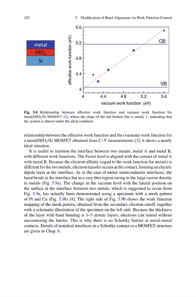
Fig. 5.8 Relationship between effective work function and vacuum work function for
metal/HfO 2 /Si MOSFET [3], where the slope of the red broken line is nearly 1, indicating that
the system is almost under the ideal condition
relationship between the effective work function and the (vacuum) work function for
a metal/HfO 2 /Si MOSFET obtained from C–V measurements [3]; it shows a nearly
ideal situation.
It is useful to mention the interface between two metals, metal A and metal B,
with different work functions. The Fermi level is aligned with the contact of metal A
with metal B. Because the electron affinity (equal to the work function for metals) is
different for the two metals, electron transfer occurs at the contact, forming an electric
dipole layer at the interface. As in the case of metal–semiconductor interfaces, the
band bends at the interface but in a very thin region owing to the large carrier density
in metals (Fig. 5.9a). The change in the vacuum level with the lateral position on
the surface at the interface between two metals, which is suggested to occur from
Fig. 5.9a, has actually been demonstrated using a specimen with a mesh pattern
of Pt and Cu (Fig. 5.9b) [4]. The right side of Fig. 5.9b shows the work function
mapping of the mesh pattern, obtained from the secondary electron cutoff, together
with a schematic illustration of the specimen on the left side. Because the thickness
of the layer with band bending is 1–3 atomic layers, electrons can tunnel without
encountering the barrier. This is why there is no Schottky barrier at metal–metal
contacts. Details of nonideal interfaces in a Schottky contact or a MOSFET structure
are given in Chap. 6.
5 Modification of Band Alignment via Work Function Control
metal
HfO 2
Si
Fig. 5.8 Relationship between effective work function and vacuum work function for
metal/HfO 2 /Si MOSFET [3], where the slope of the red broken line is nearly 1, indicating that
the system is almost under the ideal condition
relationship between the effective work function and the (vacuum) work function for
a metal/HfO 2 /Si MOSFET obtained from C–V measurements [3]; it shows a nearly
ideal situation.
It is useful to mention the interface between two metals, metal A and metal B,
with different work functions. The Fermi level is aligned with the contact of metal A
with metal B. Because the electron affinity (equal to the work function for metals) is
different for the two metals, electron transfer occurs at the contact, forming an electric
dipole layer at the interface. As in the case of metal–semiconductor interfaces, the
band bends at the interface but in a very thin region owing to the large carrier density
in metals (Fig. 5.9a). The change in the vacuum level with the lateral position on
the surface at the interface between two metals, which is suggested to occur from
Fig. 5.9a, has actually been demonstrated using a specimen with a mesh pattern
of Pt and Cu (Fig. 5.9b) [4]. The right side of Fig. 5.9b shows the work function
mapping of the mesh pattern, obtained from the secondary electron cutoff, together
with a schematic illustration of the specimen on the left side. Because the thickness
of the layer with band bending is 1–3 atomic layers, electrons can tunnel without
encountering the barrier. This is why there is no Schottky barrier at metal–metal
contacts. Details of nonideal interfaces in a Schottky contact or a MOSFET structure
are given in Chap. 6.