

5.1 Ideal Band Alignment
101
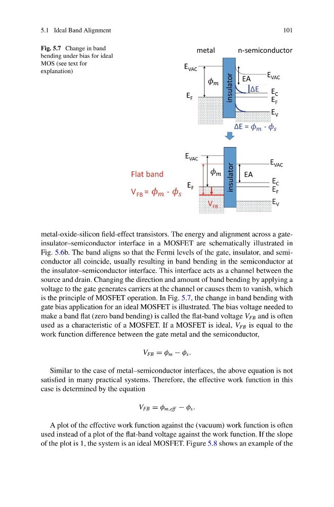
Fig. 5.7 Change in band
bending under bias for ideal
MOS (see text for
explanation)
insulator
EA
E F
E VAC
E VAC
E C
E V
E F
Flat band
V FB =
-
ΔE
EA
E F
E VAC
E VAC
E C
E V
E F
insulator
V FB
metal
n-semiconductor
ΔE =
-
metal-oxide-silicon field-effect transistors. The energy and alignment across a gateinsulator–semiconductor interface in a MOSFET are schematically illustrated in
Fig. 5.6b. The band aligns so that the Fermi levels of the gate, insulator, and semiconductor all coincide, usually resulting in band bending in the semiconductor at
the insulator–semiconductor interface. This interface acts as a channel between the
source and drain. Changing the direction and amount of band bending by applying a
voltage to the gate generates carriers at the channel or causes them to vanish, which
is the principle of MOSFET operation. In Fig. 5.7, the change in band bending with
gate bias application for an ideal MOSFET is illustrated. The bias voltage needed to
make a band flat (zero band bending) is called the flat-band voltage V FB and is often
used as a characteristic of a MOSFET. If a MOSFET is ideal, V FB is equal to the
work function difference between the gate metal and the semiconductor,
V FB = φ m − φ s .
Similar to the case of metal–semiconductor interfaces, the above equation is not
satisfied in many practical systems. Therefore, the effective work function in this
case is determined by the equation
V FB = φ m,eff − φ s .
A plot of the effective work function against the (vacuum) work function is often
used instead of a plot of the flat-band voltage against the work function. If the slope
of the plot is 1, the system is an ideal MOSFET. Figure 5.8 shows an example of the
101
Fig. 5.7 Change in band
bending under bias for ideal
MOS (see text for
explanation)
insulator
EA
E F
E VAC
E VAC
E C
E V
E F
Flat band
V FB =
-
ΔE
EA
E F
E VAC
E VAC
E C
E V
E F
insulator
V FB
metal
n-semiconductor
ΔE =
-
metal-oxide-silicon field-effect transistors. The energy and alignment across a gateinsulator–semiconductor interface in a MOSFET are schematically illustrated in
Fig. 5.6b. The band aligns so that the Fermi levels of the gate, insulator, and semiconductor all coincide, usually resulting in band bending in the semiconductor at
the insulator–semiconductor interface. This interface acts as a channel between the
source and drain. Changing the direction and amount of band bending by applying a
voltage to the gate generates carriers at the channel or causes them to vanish, which
is the principle of MOSFET operation. In Fig. 5.7, the change in band bending with
gate bias application for an ideal MOSFET is illustrated. The bias voltage needed to
make a band flat (zero band bending) is called the flat-band voltage V FB and is often
used as a characteristic of a MOSFET. If a MOSFET is ideal, V FB is equal to the
work function difference between the gate metal and the semiconductor,
V FB = φ m − φ s .
Similar to the case of metal–semiconductor interfaces, the above equation is not
satisfied in many practical systems. Therefore, the effective work function in this
case is determined by the equation
V FB = φ m,eff − φ s .
A plot of the effective work function against the (vacuum) work function is often
used instead of a plot of the flat-band voltage against the work function. If the slope
of the plot is 1, the system is an ideal MOSFET. Figure 5.8 shows an example of the