

100
5 Modification of Band Alignment via Work Function Control
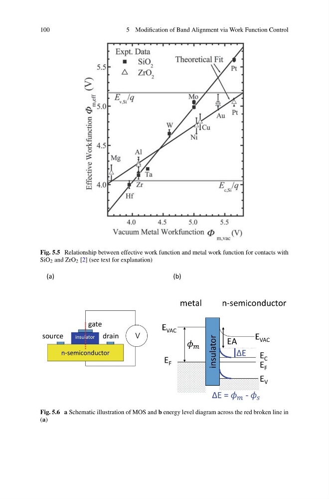
Fig. 5.5 Relationship between effective work function and metal work function for contacts with
SiO 2 and ZrO 2 [2] (see text for explanation)
(a)
(b)
n-semiconductor
insulator
source
drain
gate
ΔE =
-
insulator
EA
E F
E VAC
E VAC
E C
E V
E F
ΔE
metal
n-semiconductor
Fig. 5.6 a Schematic illustration of MOS and b energy level diagram across the red broken line in
(a)
5 Modification of Band Alignment via Work Function Control
Fig. 5.5 Relationship between effective work function and metal work function for contacts with
SiO 2 and ZrO 2 [2] (see text for explanation)
(a)
(b)
n-semiconductor
insulator
source
drain
gate
ΔE =
-
insulator
EA
E F
E VAC
E VAC
E C
E V
E F
ΔE
metal
n-semiconductor
Fig. 5.6 a Schematic illustration of MOS and b energy level diagram across the red broken line in
(a)