

52
M. Hiramoto
3.3 Vertical Junctions
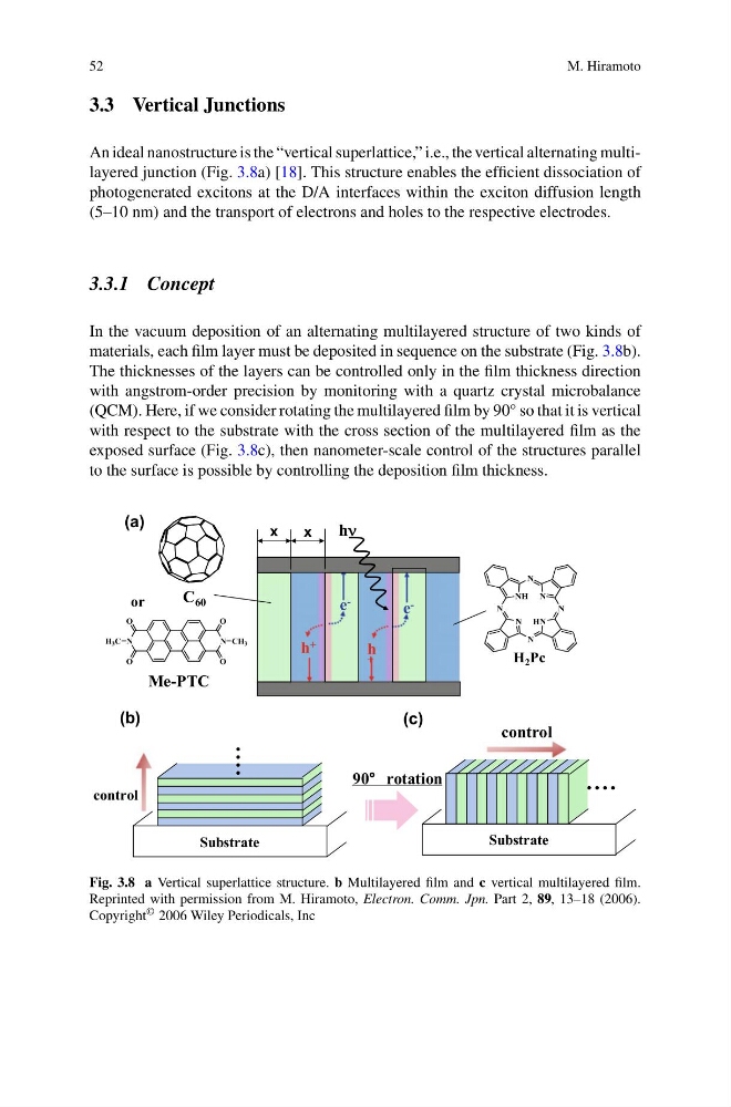
An ideal nanostructure is the “vertical superlattice,” i.e., the vertical alternating multilayered junction (Fig. 3.8a) [18]. This structure enables the efficient dissociation of
photogenerated excitons at the D/A interfaces within the exciton diffusion length
(5–10 nm) and the transport of electrons and holes to the respective electrodes.
3.3.1 Concept
In the vacuum deposition of an alternating multilayered structure of two kinds of
materials, each film layer must be deposited in sequence on the substrate (Fig. 3.8b).
The thicknesses of the layers can be controlled only in the film thickness direction
with angstrom-order precision by monitoring with a quartz crystal microbalance
(QCM). Here, if we consider rotating the multilayered film by 90° so that it is vertical
with respect to the substrate with the cross section of the multilayered film as the
exposed surface (Fig. 3.8c), then nanometer-scale control of the structures parallel
to the surface is possible by controlling the deposition film thickness.
h
H 2 Pc
NH
N
N
N
N
N
HN
N
C 60
h +
h
+
e -
e -
(a)
control
90 rotation
Substrate
Substrate
control
(c)
(b)
x
x
N
N
O
O
O
O
CH 3
H 3 C
Me-PTC
or
Fig. 3.8 a Vertical superlattice structure. b Multilayered film and c vertical multilayered film.
Reprinted with permission from M. Hiramoto, Electron. Comm. Jpn. Part 2, 89, 13–18 (2006).
Copyright © 2006 Wiley Periodicals, Inc
M. Hiramoto
3.3 Vertical Junctions
An ideal nanostructure is the “vertical superlattice,” i.e., the vertical alternating multilayered junction (Fig. 3.8a) [18]. This structure enables the efficient dissociation of
photogenerated excitons at the D/A interfaces within the exciton diffusion length
(5–10 nm) and the transport of electrons and holes to the respective electrodes.
3.3.1 Concept
In the vacuum deposition of an alternating multilayered structure of two kinds of
materials, each film layer must be deposited in sequence on the substrate (Fig. 3.8b).
The thicknesses of the layers can be controlled only in the film thickness direction
with angstrom-order precision by monitoring with a quartz crystal microbalance
(QCM). Here, if we consider rotating the multilayered film by 90° so that it is vertical
with respect to the substrate with the cross section of the multilayered film as the
exposed surface (Fig. 3.8c), then nanometer-scale control of the structures parallel
to the surface is possible by controlling the deposition film thickness.
h
H 2 Pc
NH
N
N
N
N
N
HN
N
C 60
h +
h
+
e -
e -
(a)
control
90 rotation
Substrate
Substrate
control
(c)
(b)
x
x
N
N
O
O
O
O
CH 3
H 3 C
Me-PTC
or
Fig. 3.8 a Vertical superlattice structure. b Multilayered film and c vertical multilayered film.
Reprinted with permission from M. Hiramoto, Electron. Comm. Jpn. Part 2, 89, 13–18 (2006).
Copyright © 2006 Wiley Periodicals, Inc