

3 Percolation Toward Lateral Junctions
53
3.3.2 Cell Fabrication
Regarding photoelectric conversion, when a vertical superlattice structure (Fig. 3.8a)
consisting of alternating perylene pigment (C 60 , Fig. 3.8a) layers acting as acceptor
molecules and metal-free phthalocyanine (H 2 Pc, Fig. 3.8a) layers acting as donor
molecules is exposed to light, efficient charge separation occurs at the interface of
the D/A organic semiconductors. Further, the photogenerated electrons and holes are
transported such that they are spatially separated.
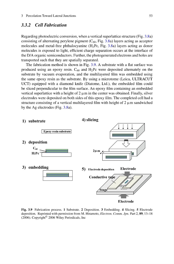
The fabrication method is shown in Fig. 3.9. A substrate with a flat surface was
produced using an epoxy resin. C 60 and H 2 Pc were deposited alternately on the
substrate by vacuum evaporation, and the multilayered film was embedded using
the same epoxy resin as the substrate. By using a microtome (Leica, ULTRACUT
UCT) equipped with a diamond knife (Diatome, Ltd.), the embedded film could
be sliced perpendicular to the film surface. An epoxy film containing an embedded
vertical superlattice with a height of 2 μm in the center was obtained. Finally, silver
electrodes were deposited on both sides of this epoxy film. The completed cell had a
structure consisting of a vertical multilayered film with height of 2 μm sandwiched
by the Ag electrodes (Fig. 3.8a).
Stage
Electrode
Conductive tape
Electrode
5) Electrode deposition
2 m
Epoxy resin substrate
1) substrate
2) deposition
3) embedding
4) slicing
C 60
H2Pc
Fig. 3.9 Fabrication process. 1 Substrate. 2 Deposition. 3 Embedding. 4 Slicing. 5 Electrode
deposition. Reprinted with permission from M. Hiramoto, Electron. Comm. Jpn. Part 2, 89, 13–18
(2006). Copyright © 2006 Wiley Periodicals, Inc
53
3.3.2 Cell Fabrication
Regarding photoelectric conversion, when a vertical superlattice structure (Fig. 3.8a)
consisting of alternating perylene pigment (C 60 , Fig. 3.8a) layers acting as acceptor
molecules and metal-free phthalocyanine (H 2 Pc, Fig. 3.8a) layers acting as donor
molecules is exposed to light, efficient charge separation occurs at the interface of
the D/A organic semiconductors. Further, the photogenerated electrons and holes are
transported such that they are spatially separated.
The fabrication method is shown in Fig. 3.9. A substrate with a flat surface was
produced using an epoxy resin. C 60 and H 2 Pc were deposited alternately on the
substrate by vacuum evaporation, and the multilayered film was embedded using
the same epoxy resin as the substrate. By using a microtome (Leica, ULTRACUT
UCT) equipped with a diamond knife (Diatome, Ltd.), the embedded film could
be sliced perpendicular to the film surface. An epoxy film containing an embedded
vertical superlattice with a height of 2 μm in the center was obtained. Finally, silver
electrodes were deposited on both sides of this epoxy film. The completed cell had a
structure consisting of a vertical multilayered film with height of 2 μm sandwiched
by the Ag electrodes (Fig. 3.8a).
Stage
Electrode
Conductive tape
Electrode
5) Electrode deposition
2 m
Epoxy resin substrate
1) substrate
2) deposition
3) embedding
4) slicing
C 60
H2Pc
Fig. 3.9 Fabrication process. 1 Substrate. 2 Deposition. 3 Embedding. 4 Slicing. 5 Electrode
deposition. Reprinted with permission from M. Hiramoto, Electron. Comm. Jpn. Part 2, 89, 13–18
(2006). Copyright © 2006 Wiley Periodicals, Inc