

3 Percolation Toward Lateral Junctions
49
3.2.3 p-i-n Cells
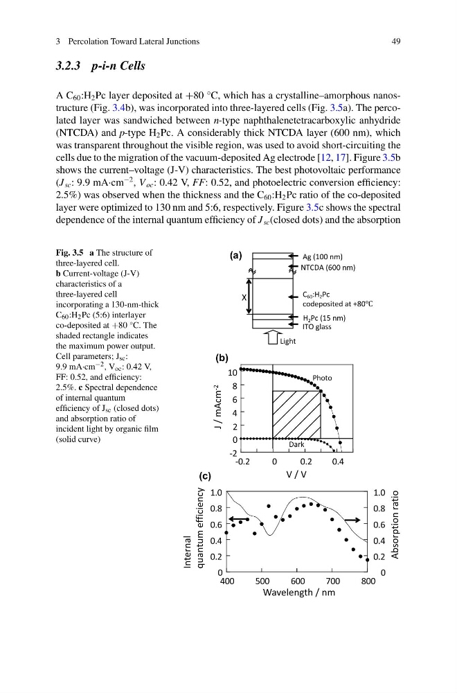
A C 60 :H 2 Pc layer deposited at +80 °C, which has a crystalline–amorphous nanostructure (Fig. 3.4b), was incorporated into three-layered cells (Fig. 3.5a). The percolated layer was sandwiched between n-type naphthalenetetracarboxylic anhydride
(NTCDA) and p-type H 2 Pc. A considerably thick NTCDA layer (600 nm), which
was transparent throughout the visible region, was used to avoid short-circuiting the
cells due to the migration of the vacuum-deposited Ag electrode [12, 17]. Figure 3.5b
shows the current–voltage (J-V) characteristics. The best photovoltaic performance
(J sc : 9.9 mA·cm
−2 , V oc : 0.42 V, FF: 0.52, and photoelectric conversion efficiency:
2.5%) was observed when the thickness and the C 60 :H 2 Pc ratio of the co-deposited
layer were optimized to 130 nm and 5:6, respectively. Figure 3.5c shows the spectral
dependence of the internal quantum efficiency of J sc (closed dots) and the absorption
Fig. 3.5 a The structure of
three-layered cell.
b Current-voltage (J-V)
characteristics of a
three-layered cell
incorporating a 130-nm-thick
C 60 :H 2 Pc (5:6) interlayer
co-deposited at +80 °C. The
shaded rectangle indicates
the maximum power output.
Cell parameters; J sc :
9.9 mA·cm −2 , V oc : 0.42 V,
FF: 0.52, and efficiency:
2.5%. c Spectral dependence
of internal quantum
efficiency of J sc (closed dots)
and absorption ratio of
incident light by organic film
(solid curve)
(a)
(b)
(c)
49
3.2.3 p-i-n Cells
A C 60 :H 2 Pc layer deposited at +80 °C, which has a crystalline–amorphous nanostructure (Fig. 3.4b), was incorporated into three-layered cells (Fig. 3.5a). The percolated layer was sandwiched between n-type naphthalenetetracarboxylic anhydride
(NTCDA) and p-type H 2 Pc. A considerably thick NTCDA layer (600 nm), which
was transparent throughout the visible region, was used to avoid short-circuiting the
cells due to the migration of the vacuum-deposited Ag electrode [12, 17]. Figure 3.5b
shows the current–voltage (J-V) characteristics. The best photovoltaic performance
(J sc : 9.9 mA·cm
−2 , V oc : 0.42 V, FF: 0.52, and photoelectric conversion efficiency:
2.5%) was observed when the thickness and the C 60 :H 2 Pc ratio of the co-deposited
layer were optimized to 130 nm and 5:6, respectively. Figure 3.5c shows the spectral
dependence of the internal quantum efficiency of J sc (closed dots) and the absorption
Fig. 3.5 a The structure of
three-layered cell.
b Current-voltage (J-V)
characteristics of a
three-layered cell
incorporating a 130-nm-thick
C 60 :H 2 Pc (5:6) interlayer
co-deposited at +80 °C. The
shaded rectangle indicates
the maximum power output.
Cell parameters; J sc :
9.9 mA·cm −2 , V oc : 0.42 V,
FF: 0.52, and efficiency:
2.5%. c Spectral dependence
of internal quantum
efficiency of J sc (closed dots)
and absorption ratio of
incident light by organic film
(solid curve)
(a)
(b)
(c)