

36
M. Hiramoto
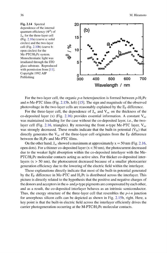
Fig. 2.14 Spectral
dependence of the internal
quantum efficiency ( 0 ) of
J sc for the three-layer cell
(Fig. 2.10a) (curve a: solid
circles) and the two-layer
cell (Fig. 2.10b) (curve b:
open circles) for the
Me-PTC/H 2 Pc system.
Monochromatic light was
irradiated through the ITO
glass substrate. Reproduced
with permission from [11].
Copyright 1992 AIP
Publishing
For the two-layer cell, the organic p-n heterojunction is formed between p-H 2 Pc
and n-Me-PTC films (Fig. 2.15b, left) [15]. The sign and magnitude of the observed
photovoltage in the two-layer cells are reasonably explained by the E F difference.
For the three-layer cell, the dependence of J sc and V oc on the thickness of the
co-deposited layer (x) (Fig. 2.16) provides essential information. A constant V oc
was maintained including for the case without the co-deposited layer, i.e., the twolayer cell (Fig. 2.16, triangles). By removing the front n-type Me-PTC layer, V oc
was strongly decreased. These results indicate that the built-in potential (V bi ) that
directly generates the V oc of the three-layer cell originates from the E F difference
between the H 2 Pc and Me-PTC films.
On the other hand, J sc showed a maximum at approximately x = 50 nm (Fig. 2.16,
open dots). For a thinner co-deposited layer (x < 50 nm), the photocurrent decreased
due to the weaker light absorption within the co-deposited interlayer with the MePTC/H 2 Pc molecular contacts acting as active sites. For thicker co-deposited interlayers (x > 50 nm), the photocurrent decreased because of a smaller photocarrier
generation efficiency due to the lowering of the electric field within the interlayer.
These explanations directly indicate that most of the built-in potential generated
by the E F difference in Me-PTC and H 2 Pc is distributed across the interlayer. This
picture is directly related to the hypothesis that the positive and negative charges of
the donors and acceptors in the n- and p-type pigments are compensated by each other,
and as a result, the co-deposited interlayer behaves as an intrinsic semiconductor.
Thus, the energy structure of the three-layer cell that resembles the p-i-n junction
for amorphous silicon cells can be depicted as shown in Fig. 2.15b, right. Here, a
key point is that the built-in electric field across the interlayer efficiently drives the
carrier photogeneration occurring at the M-PTC/H 2 Pc molecular contacts.
M. Hiramoto
Fig. 2.14 Spectral
dependence of the internal
quantum efficiency ( 0 ) of
J sc for the three-layer cell
(Fig. 2.10a) (curve a: solid
circles) and the two-layer
cell (Fig. 2.10b) (curve b:
open circles) for the
Me-PTC/H 2 Pc system.
Monochromatic light was
irradiated through the ITO
glass substrate. Reproduced
with permission from [11].
Copyright 1992 AIP
Publishing
For the two-layer cell, the organic p-n heterojunction is formed between p-H 2 Pc
and n-Me-PTC films (Fig. 2.15b, left) [15]. The sign and magnitude of the observed
photovoltage in the two-layer cells are reasonably explained by the E F difference.
For the three-layer cell, the dependence of J sc and V oc on the thickness of the
co-deposited layer (x) (Fig. 2.16) provides essential information. A constant V oc
was maintained including for the case without the co-deposited layer, i.e., the twolayer cell (Fig. 2.16, triangles). By removing the front n-type Me-PTC layer, V oc
was strongly decreased. These results indicate that the built-in potential (V bi ) that
directly generates the V oc of the three-layer cell originates from the E F difference
between the H 2 Pc and Me-PTC films.
On the other hand, J sc showed a maximum at approximately x = 50 nm (Fig. 2.16,
open dots). For a thinner co-deposited layer (x < 50 nm), the photocurrent decreased
due to the weaker light absorption within the co-deposited interlayer with the MePTC/H 2 Pc molecular contacts acting as active sites. For thicker co-deposited interlayers (x > 50 nm), the photocurrent decreased because of a smaller photocarrier
generation efficiency due to the lowering of the electric field within the interlayer.
These explanations directly indicate that most of the built-in potential generated
by the E F difference in Me-PTC and H 2 Pc is distributed across the interlayer. This
picture is directly related to the hypothesis that the positive and negative charges of
the donors and acceptors in the n- and p-type pigments are compensated by each other,
and as a result, the co-deposited interlayer behaves as an intrinsic semiconductor.
Thus, the energy structure of the three-layer cell that resembles the p-i-n junction
for amorphous silicon cells can be depicted as shown in Fig. 2.15b, right. Here, a
key point is that the built-in electric field across the interlayer efficiently drives the
carrier photogeneration occurring at the M-PTC/H 2 Pc molecular contacts.