

8 Open-Circuit Voltage in Organic Solar Cells
203
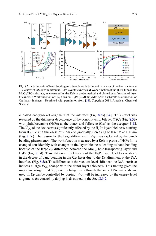
Fig. 8.5 a Schematic of band bending near interfaces. b Schematic diagram of device structure. c
J-V curves of OSCs with different H 2 Pc layer thicknesses. d Work function of the H 2 Pc film on the
MoO 3 /ITO substrate, as measured by the Kelvin probe method and plotted as a function of layer
thickness. e Work function of C 60 films on H 2 Pc (2–70 nm)/MoO 3 /ITO substrate as a function of
C 60 layer thickness. Reprinted with permission from [18]. Copyright 2018, American Chemical
Society
is called energy-level alignment at the interface (Fig. 8.5a) [26]. This effect was
revealed by the thickness dependence of the donor layer in bilayer OSCs (Fig. 8.5b)
with phthalocyanine (H 2 Pc) as the donor and fullerene (C 60 ) as the acceptor [18].
The V OC of the device was significantly affected by the H 2 Pc layer thickness, starting
from 0.20 V at a thickness of 2 nm and gradually increasing to 0.49 V at 100 nm
(Fig. 8.5c). The reason for the large difference in V OC was explained by the bandbending phenomenon. The work function measured by a Kelvin probe of H 2 Pc films
changed considerably with changes in the layer thickness, leading to band bending
because of the large E F difference between the MoO 3 hole-transporting layer and
H 2 Pc (Fig. 8.5d). Thus, different thicknesses of the H 2 Pc layer lead to variations
in the degree of band bending in the C 60 layer due to the E F alignment at the D/A
interface (Fig. 8.5e). This difference in the vacuum-level shift near the D/A interface
induces a large V OC change with the donor layer thickness. This finding gives the
important insight that V OC could change even though the same D/A materials are
used. If E F can be controlled by doping, V OC will be increased by the energy-level
alignment. E F control by doping is discussed in the Sect.8.3.2.
203
Fig. 8.5 a Schematic of band bending near interfaces. b Schematic diagram of device structure. c
J-V curves of OSCs with different H 2 Pc layer thicknesses. d Work function of the H 2 Pc film on the
MoO 3 /ITO substrate, as measured by the Kelvin probe method and plotted as a function of layer
thickness. e Work function of C 60 films on H 2 Pc (2–70 nm)/MoO 3 /ITO substrate as a function of
C 60 layer thickness. Reprinted with permission from [18]. Copyright 2018, American Chemical
Society
is called energy-level alignment at the interface (Fig. 8.5a) [26]. This effect was
revealed by the thickness dependence of the donor layer in bilayer OSCs (Fig. 8.5b)
with phthalocyanine (H 2 Pc) as the donor and fullerene (C 60 ) as the acceptor [18].
The V OC of the device was significantly affected by the H 2 Pc layer thickness, starting
from 0.20 V at a thickness of 2 nm and gradually increasing to 0.49 V at 100 nm
(Fig. 8.5c). The reason for the large difference in V OC was explained by the bandbending phenomenon. The work function measured by a Kelvin probe of H 2 Pc films
changed considerably with changes in the layer thickness, leading to band bending
because of the large E F difference between the MoO 3 hole-transporting layer and
H 2 Pc (Fig. 8.5d). Thus, different thicknesses of the H 2 Pc layer lead to variations
in the degree of band bending in the C 60 layer due to the E F alignment at the D/A
interface (Fig. 8.5e). This difference in the vacuum-level shift near the D/A interface
induces a large V OC change with the donor layer thickness. This finding gives the
important insight that V OC could change even though the same D/A materials are
used. If E F can be controlled by doping, V OC will be increased by the energy-level
alignment. E F control by doping is discussed in the Sect.8.3.2.