

204
S. Izawa
8.3.2 Doping for Controlling Open-Circuit Voltage
in Organic Solar Cells
Doping, addition of trace amounts of p-type and n-type impurities to form a pn
junction, is the central technology in inorganic solar cells. The doping effect at
the D/A interface was investigated by co-evaporating a p-type (MoO 3 ) or n-type
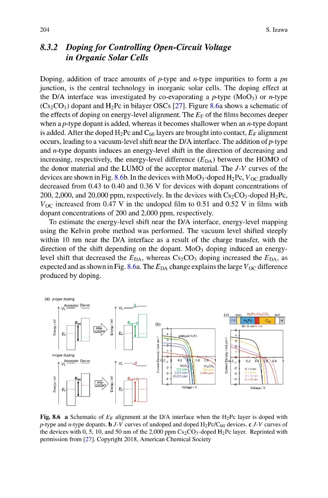
(Cs 2 CO 3 ) dopant and H 2 Pc in bilayer OSCs [27]. Figure 8.6a shows a schematic of
the effects of doping on energy-level alignment. The E F of the films becomes deeper
when a p-type dopant is added, whereas it becomes shallower when an n-type dopant
is added. After the doped H 2 Pc and C 60 layers are brought into contact, E F alignment
occurs, leading to a vacuum-level shift near the D/A interface. The addition of p-type
and n-type dopants induces an energy-level shift in the direction of decreasing and
increasing, respectively, the energy-level difference (E DA ) between the HOMO of
the donor material and the LUMO of the acceptor material. The J-V curves of the
devices are shown in Fig. 8.6b. In the devices with MoO 3 -doped H 2 Pc, V OC gradually
decreased from 0.43 to 0.40 and 0.36 V for devices with dopant concentrations of
200, 2,000, and 20,000 ppm, respectively. In the devices with Cs 2 CO 3 -doped H 2 Pc,
V OC increased from 0.47 V in the undoped film to 0.51 and 0.52 V in films with
dopant concentrations of 200 and 2,000 ppm, respectively.
To estimate the energy-level shift near the D/A interface, energy-level mapping
using the Kelvin probe method was performed. The vacuum level shifted steeply
within 10 nm near the D/A interface as a result of the charge transfer, with the
direction of the shift depending on the dopant. MoO 3 doping induced an energylevel shift that decreased the E DA , whereas Cs 2 CO 3 doping increased the E DA , as
expected and as shown in Fig. 8.6a. The E DA change explains the large V OC difference
produced by doping.
Fig. 8.6 a Schematic of E F alignment at the D/A interface when the H 2 Pc layer is doped with
p-type and n-type dopants. b J-V curves of undoped and doped H 2 Pc/C 60 devices. c J-V curves of
the devices with 0, 5, 10, and 50 nm of the 2,000 ppm Cs 2 CO 3 -doped H 2 Pc layer. Reprinted with
permission from [27]. Copyright 2018, American Chemical Society
S. Izawa
8.3.2 Doping for Controlling Open-Circuit Voltage
in Organic Solar Cells
Doping, addition of trace amounts of p-type and n-type impurities to form a pn
junction, is the central technology in inorganic solar cells. The doping effect at
the D/A interface was investigated by co-evaporating a p-type (MoO 3 ) or n-type
(Cs 2 CO 3 ) dopant and H 2 Pc in bilayer OSCs [27]. Figure 8.6a shows a schematic of
the effects of doping on energy-level alignment. The E F of the films becomes deeper
when a p-type dopant is added, whereas it becomes shallower when an n-type dopant
is added. After the doped H 2 Pc and C 60 layers are brought into contact, E F alignment
occurs, leading to a vacuum-level shift near the D/A interface. The addition of p-type
and n-type dopants induces an energy-level shift in the direction of decreasing and
increasing, respectively, the energy-level difference (E DA ) between the HOMO of
the donor material and the LUMO of the acceptor material. The J-V curves of the
devices are shown in Fig. 8.6b. In the devices with MoO 3 -doped H 2 Pc, V OC gradually
decreased from 0.43 to 0.40 and 0.36 V for devices with dopant concentrations of
200, 2,000, and 20,000 ppm, respectively. In the devices with Cs 2 CO 3 -doped H 2 Pc,
V OC increased from 0.47 V in the undoped film to 0.51 and 0.52 V in films with
dopant concentrations of 200 and 2,000 ppm, respectively.
To estimate the energy-level shift near the D/A interface, energy-level mapping
using the Kelvin probe method was performed. The vacuum level shifted steeply
within 10 nm near the D/A interface as a result of the charge transfer, with the
direction of the shift depending on the dopant. MoO 3 doping induced an energylevel shift that decreased the E DA , whereas Cs 2 CO 3 doping increased the E DA , as
expected and as shown in Fig. 8.6a. The E DA change explains the large V OC difference
produced by doping.
Fig. 8.6 a Schematic of E F alignment at the D/A interface when the H 2 Pc layer is doped with
p-type and n-type dopants. b J-V curves of undoped and doped H 2 Pc/C 60 devices. c J-V curves of
the devices with 0, 5, 10, and 50 nm of the 2,000 ppm Cs 2 CO 3 -doped H 2 Pc layer. Reprinted with
permission from [27]. Copyright 2018, American Chemical Society