

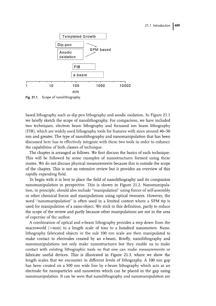
based lithography such as dip pen lithography and anodic oxidation. In Figure 21.1
we briefly sketch the scope of nanolithography. For comparison, we have included
two techniques, electron beam lithography and focussed ion beam lithography
(FIB), which are widely used lithography tools for features with sizes around 40–50
nm and greater. The type of nanolithography and nanomanipulation that has been
discussed here has to effectively integrate with these two tools in order to enhance
the capabilities of both classes of technique.
The chapter is arranged as follows. We first discuss the basics of each technique.
This will be followed by some examples of nanostructures formed using these
routes. We do not discuss physical measurements because this is outside the scope
of the chapter. This is not an extensive review but it provides an overview of this
rapidly expanding field.
To begin with it is best to place the field of nanolithography and its companion
nanomanipulation in perspective. This is shown in Figure 21.2. Nanomanipulation, in principle, should also include ‘‘manipulation’’ using forces of self-assembly
or other chemical forces and manipulations using optical tweezers. However, the
word ‘‘nanomanipulation’’ is often used in a limited context where a SPM tip is
used for manipulation of a nano-object. We stick to this definition, partly to reduce
the scope of the review and partly because other manipulations are not in the area
of expertise of the author.
A combination of optical and e-beam lithography provides a step down from the
macroworld (@mm) to a length scale of tens to a hundred nanometers. Nanolithography fabricated objects in the sub 100 nm scale are then manipulated to
make contact to electrodes created by an e-beam. Briefly, nanolithography and
nanomanipulations not only make nanostructures but they enable us to make
contact with existing lithographic tools so that one can make measurements or
fabricate useful devices. This is illustrated in Figure 21.3, where we show the
length scales that we encounter in different levels of lithography. A 100 nm gap
has been created on a 500 nm wide line by e-beam lithography which acts as an
electrode for nanoparticles and nanowires which can be placed in the gap using
nanomanipulation. It can be seen that nanolithography and nanomanipulation are
Fig. 21.1. Scope of nanolithography.
21.1 Introduction 689