

The onset potential at which the electrochromic effect is observed corresponds to
the flat band potential of the corresponding semiconductor and is dependent on
the pH of the medium. With increasing pH the onset of the electrochromic effect
was found to shift to more negative potentials [148, 149]. By monitoring the optical
absorbance, Fitzmaurice and his coworkers [148–152] have determined the flatband potentials of nanostructured films of TiO 2 and GaAs and the extinction
coefficient of the trapped electrons. On the other hand ZnO [153], SnO 2 [154], and
CdS [155] films exhibit bleaching at potentials more negative than the flat band
potential.
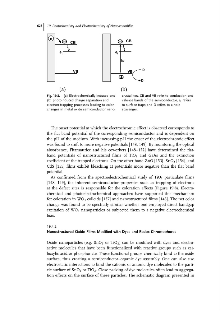
As confirmed from the spectroelectrochemical study of TiO 2 particulate films
[148, 149], the inherent semiconductor properties such as trapping of electrons
at the defect sites is responsible for the coloration effects (Figure 19.8). Electrochemical and photoelectrochemical approaches have supported this mechanism
for coloration in WO 3 colloids [137] and nanostructured films [143]. The net color
change was found to be spectrally similar whether one employed direct bandgap
excitation of WO 3 nanoparticles or subjected them to a negative electrochemical
bias.
19.4.2
Nanostructured Oxide Films Modified with Dyes and Redox Chromophores
Oxide nanoparticles (e.g. SnO 2 or TiO 2 ) can be modified with dyes and electroactive molecules that have been functionalized with reactive groups such as carboxylic acid or phosphonate. These functional groups chemically bind to the oxide
surface, thus creating a semiconductor–organic dye assembly. One can also use
electrostatic interactions to bind the cationic or anionic dye molecules to the particle surface of SnO 2 or TiO 2 . Close packing of dye molecules often lead to aggregation effects on the surface of these particles. The schematic diagram presented in
e t
VB
CB
hn
D
D +
e t
VB
CB
e
(a)
(b)
Fig. 19.8. (a) Electrochemically induced and
(b) photoinduced charge separation and
electron trapping processes leading to color
changes in metal oxide semiconductor nanocrystallites. CB and VB refer to conduction and
valence bands of the semiconductor, e t refers
to surface traps and D refers to a hole
scavenger.
19 Photochemistry and Electrochemistry of Nanoassemblies
628