

of colours within the etching solution (known as Fabry–Pe ´rot fringes) and the
evolution of dihydrogen gas, the reduction product, from the platinum loop cathode. Despite preparation in air, the surface of freshly etched porous silicon is
hydride-terminated and not oxide-terminated, resulting in a hydrophobic and
chemically homogeneous interface. Like flat crystalline silicon, hydride-passivated
porous silicon oxidizes readily under ambient conditions to form a thin, insulating
oxide overlayer, demonstrating a common reactivity for these two materials. However, porous silicon has a number of novel properties that distinguish it from its
parent substrate, illustrating the unique nature of the silicon nanocrystallites and
making this material a new, possibly complementary component for silicon-based
technologies.
The physical and chemical properties of porous silicon can be characterized by
a variety of analytical techniques. Electron and scanning probe microscopies are
employed to directly image the structural elements of the silicon matrix and
acquire information regarding size, shape, and orientation of the nanocrystalline
domains. The dimensions of the silicon nanocrystallites (10
0 –10
1 nm) are well
within the resolution of transmission electron microscopy (TEM) [14]; however,
the inherent fragility of these domains requires exceptional caution in the preparation of microscopy samples. Tightly controlled ion milling is the most successful
means of preparing exceptionally thin specimens without inflicting significant
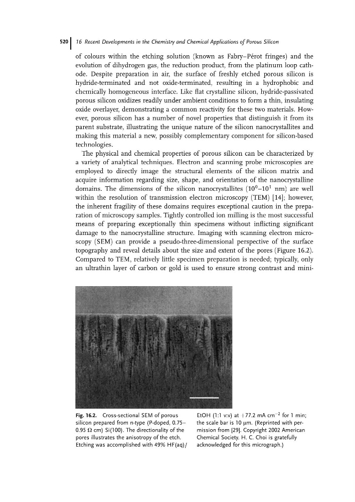
damage to the nanocrystalline structure. Imaging with scanning electron microscopy (SEM) can provide a pseudo-three-dimensional perspective of the surface
topography and reveal details about the size and extent of the pores (Figure 16.2).
Compared to TEM, relatively little specimen preparation is needed; typically, only
an ultrathin layer of carbon or gold is used to ensure strong contrast and miniFig. 16.2. Cross-sectional SEM of porous
silicon prepared from n-type (P-doped, 0.75–
0.95 W cm) Si(100). The directionality of the
pores illustrates the anisotropy of the etch.
Etching was accomplished with 49% HF(aq)/
EtOH (1:1 v:v) at þ77.2 mA cm
À2 for 1 min;
the scale bar is 10 mm. (Reprinted with permission from [29]. Copyright 2002 American
Chemical Society. H. C. Choi is gratefully
acknowledged for this micrograph.)
16 Recent Developments in the Chemistry and Chemical Applications of Porous Silicon
520