

cal [8], or electrochemical [9] etching of flat, single-crystal silicon with fluoride
solutions. Although chemical (‘‘stain’’) etching of flat silicon is easily accomplished
owing to its open-circuit, relatively simple experimental apparatus, porous silicon
prepared in this fashion exhibits substantial variability in its properties from sample to sample. Galvanostatic anodization of flat silicon is the method most often
employed to fabricate porous silicon since greater reliability and selectivity in the
product can be achieved. Aqueous HF in ethanol is the etchant chiefly used; the
ethanol is added as a surfactant to reduce the surface tension of the etching solution and to enable full wetting of the silicon substrate. Anodization is completed at
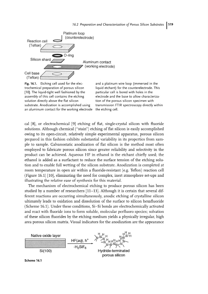
room temperature in open air within a fluoride-resistant (e.g. Teflon) reaction cell
(Figure 16.1) [10], eliminating the need for complex, inert atmosphere set-ups and
illustrating the relative ease of synthesis for this material.
The mechanism of electrochemical etching to produce porous silicon has been
studied by a number of researchers [11–13]. Although it is certain that several different reactions are occurring simultaneously, anodic etching of crystalline silicon
ultimately leads to oxidation and dissolution of the surface to silicon hexafluoride
(Scheme 16.1). Under these conditions, SiaSi bonds are electrochemically activated
and react with fluoride ions to form soluble, molecular perfluoro species; solvation
of these silicon fluorides by the etching medium yields a physically irregular, high
area porous silicon matrix. Visual indicators for the anodization are the appearance
Fig. 16.1. Etching cell used for the electrochemical preparation of porous silicon
[10]. The liquid-tight well fashioned by the
assembly of this cell contains the etching
solution directly above the flat silicon
substrate. Anodization is accomplished using
an aluminum contact for the working electrode
and a platinum wire loop (immersed in the
liquid etchant) for the counterelectrode. This
particular cell is bored with holes in the
electrode and the base to allow characterization of the porous silicon specimen with
transmission FTIR spectroscopy directly within
the etching cell.
Scheme 16.1
16.2 Preparation and Characterization of Porous Silicon Substrates 519