

strates. Hexanedithiol is approximately 10 A ˚ long and thus allows the electrons to
tunnel from the metal substrate to the nanocrystals, thus maintaining charge
neutrality. A different method to avoid charging was employed by Nanda et al. [99,
100], by mixing nanocrystals with graphite powders to provide a conducting matrix. In some cases, for very large band gap nanocrystals, graphite powder could
not remove the charging effect completely. In such cases, a low energy electron
flood gun was used to replenish the lost electrons.
11.6.1
Core Level Photoemission
Detailed investigations on CdS and ZnS nanocrystals have been carried out by different groups [99–101]. Nanda et al. [99, 100] studied various sized nanocrystals of
CdS and ZnS capped with thioglycerol. Al-K a radiation (hn ¼ 1486:6 eV) was used
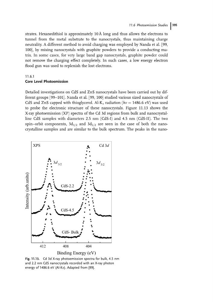
to probe the electronic structure of these nanocrystals. Figure 11.13 shows the
X-ray photoemission (XP) spectra of the Cd 3d regions from bulk and nanocrystalline CdS samples with diameters 2.5 nm (CdS-I) and 4.5 nm (CdS-II). The two
spin–orbit components, 3d 3=2 and 3d 5=2 are seen in the case of both the nanocrystalline samples and are similar to the bulk spectrum. The peaks in the nano412
408
404
XPS
Cd 3d
3d 3/2
3d 5/2
CdS- Bulk
CdS-4.5
CdS-2.2
Intensity (arb.units)
Binding Energy (eV)
Fig. 11.13. Cd 3d X-ray photoemission spectra for bulk, 4.5 nm
and 2.2 nm CdS nanocrystals recorded with an X-ray photon
energy of 1486.6 eV (Al-Ka). Adapted from [99].
11.6 Photoemission Studies 395
tunnel from the metal substrate to the nanocrystals, thus maintaining charge
neutrality. A different method to avoid charging was employed by Nanda et al. [99,
100], by mixing nanocrystals with graphite powders to provide a conducting matrix. In some cases, for very large band gap nanocrystals, graphite powder could
not remove the charging effect completely. In such cases, a low energy electron
flood gun was used to replenish the lost electrons.
11.6.1
Core Level Photoemission
Detailed investigations on CdS and ZnS nanocrystals have been carried out by different groups [99–101]. Nanda et al. [99, 100] studied various sized nanocrystals of
CdS and ZnS capped with thioglycerol. Al-K a radiation (hn ¼ 1486:6 eV) was used
to probe the electronic structure of these nanocrystals. Figure 11.13 shows the
X-ray photoemission (XP) spectra of the Cd 3d regions from bulk and nanocrystalline CdS samples with diameters 2.5 nm (CdS-I) and 4.5 nm (CdS-II). The two
spin–orbit components, 3d 3=2 and 3d 5=2 are seen in the case of both the nanocrystalline samples and are similar to the bulk spectrum. The peaks in the nano412
408
404
XPS
Cd 3d
3d 3/2
3d 5/2
CdS- Bulk
CdS-4.5
CdS-2.2
Intensity (arb.units)
Binding Energy (eV)
Fig. 11.13. Cd 3d X-ray photoemission spectra for bulk, 4.5 nm
and 2.2 nm CdS nanocrystals recorded with an X-ray photon
energy of 1486.6 eV (Al-Ka). Adapted from [99].
11.6 Photoemission Studies 395