

crystals are slightly broader and shifted to lower binding energies, which can be
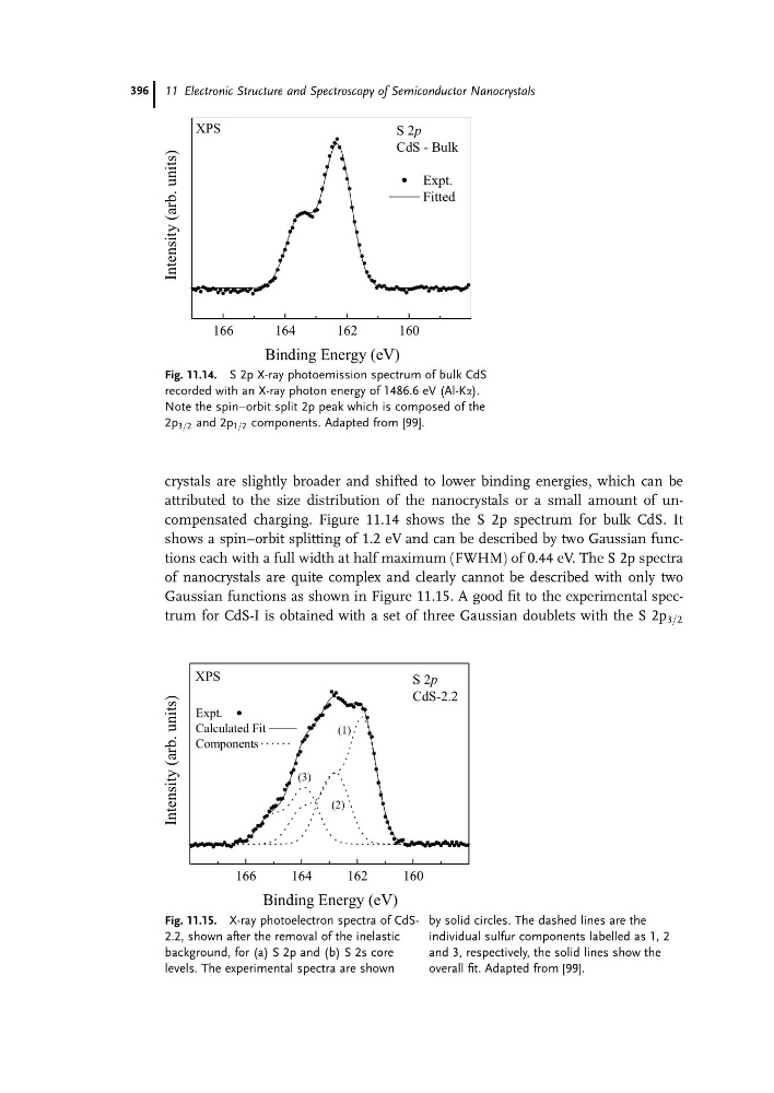
attributed to the size distribution of the nanocrystals or a small amount of uncompensated charging. Figure 11.14 shows the S 2p spectrum for bulk CdS. It
shows a spin–orbit splitting of 1.2 eV and can be described by two Gaussian functions each with a full width at half maximum (FWHM) of 0.44 eV. The S 2p spectra
of nanocrystals are quite complex and clearly cannot be described with only two
Gaussian functions as shown in Figure 11.15. A good fit to the experimental spectrum for CdS-I is obtained with a set of three Gaussian doublets with the S 2p 3=2
166
164
162
160
Intensity (arb. units)
Binding Energy (eV)
Expt.
Fitted
XPS
S 2p
CdS - Bulk
Fig. 11.14. S 2p X-ray photoemission spectrum of bulk CdS
recorded with an X-ray photon energy of 1486.6 eV (Al-Ka).
Note the spin–orbit split 2p peak which is composed of the
2p 3=2 and 2p 1=2 components. Adapted from [99].
166
164
162
160
Intensity (arb. units)
Binding Energy (eV)
Expt.
Calculated Fit
Components
XPS
(3)
(2)
(1)
S 2p
CdS-2.2
Fig. 11.15. X-ray photoelectron spectra of CdS2.2, shown after the removal of the inelastic
background, for (a) S 2p and (b) S 2s core
levels. The experimental spectra are shown
by solid circles. The dashed lines are the
individual sulfur components labelled as 1, 2
and 3, respectively, the solid lines show the
overall fit. Adapted from [99].
11 Electronic Structure and Spectroscopy of Semiconductor Nanocrystals
396
attributed to the size distribution of the nanocrystals or a small amount of uncompensated charging. Figure 11.14 shows the S 2p spectrum for bulk CdS. It
shows a spin–orbit splitting of 1.2 eV and can be described by two Gaussian functions each with a full width at half maximum (FWHM) of 0.44 eV. The S 2p spectra
of nanocrystals are quite complex and clearly cannot be described with only two
Gaussian functions as shown in Figure 11.15. A good fit to the experimental spectrum for CdS-I is obtained with a set of three Gaussian doublets with the S 2p 3=2
166
164
162
160
Intensity (arb. units)
Binding Energy (eV)
Expt.
Fitted
XPS
S 2p
CdS - Bulk
Fig. 11.14. S 2p X-ray photoemission spectrum of bulk CdS
recorded with an X-ray photon energy of 1486.6 eV (Al-Ka).
Note the spin–orbit split 2p peak which is composed of the
2p 3=2 and 2p 1=2 components. Adapted from [99].
166
164
162
160
Intensity (arb. units)
Binding Energy (eV)
Expt.
Calculated Fit
Components
XPS
(3)
(2)
(1)
S 2p
CdS-2.2
Fig. 11.15. X-ray photoelectron spectra of CdS2.2, shown after the removal of the inelastic
background, for (a) S 2p and (b) S 2s core
levels. The experimental spectra are shown
by solid circles. The dashed lines are the
individual sulfur components labelled as 1, 2
and 3, respectively, the solid lines show the
overall fit. Adapted from [99].
11 Electronic Structure and Spectroscopy of Semiconductor Nanocrystals
396