

11.6
Photoemission Studies
The semiconducting nanocrystallites are grown by colloidal chemistry routes and
obtained as free standing powders. These nanocrystals are generally coated with a
layer of an organic capping agent to arrest their growth. Performing photoemission
experiments on these semiconductor nanocrystals is a challenging task as the
photoemission process causes charging up of the non-conducting samples due to
the continuous removal or emission of electrons. To avoid the problem of charging,
various techniques have been employed. For example, Bowen Katari et al. [98] used
hexanedithiol as a linker to attach CdSe nanocrystals to gold or aluminum sub0.0
0.4
0.8
-0.8
-0.4
0.0
0.4
0.8
-4 -2 0
2
4
-0.8
-0.4
0.0
0.4
0.8
-0.8
-0.4
0.0
0.1
0.2
-4 -2 0
2
4
-0.4
-0.2
(c) 12.1 Å
total
As p
(b) 18.5 Å
total
As p
(a) 25.0 Å
total
As p
Density of states (arb. units)
Energy (eV)
(d) Mn d
25.0 Å
18.5 Å
12.1 Å
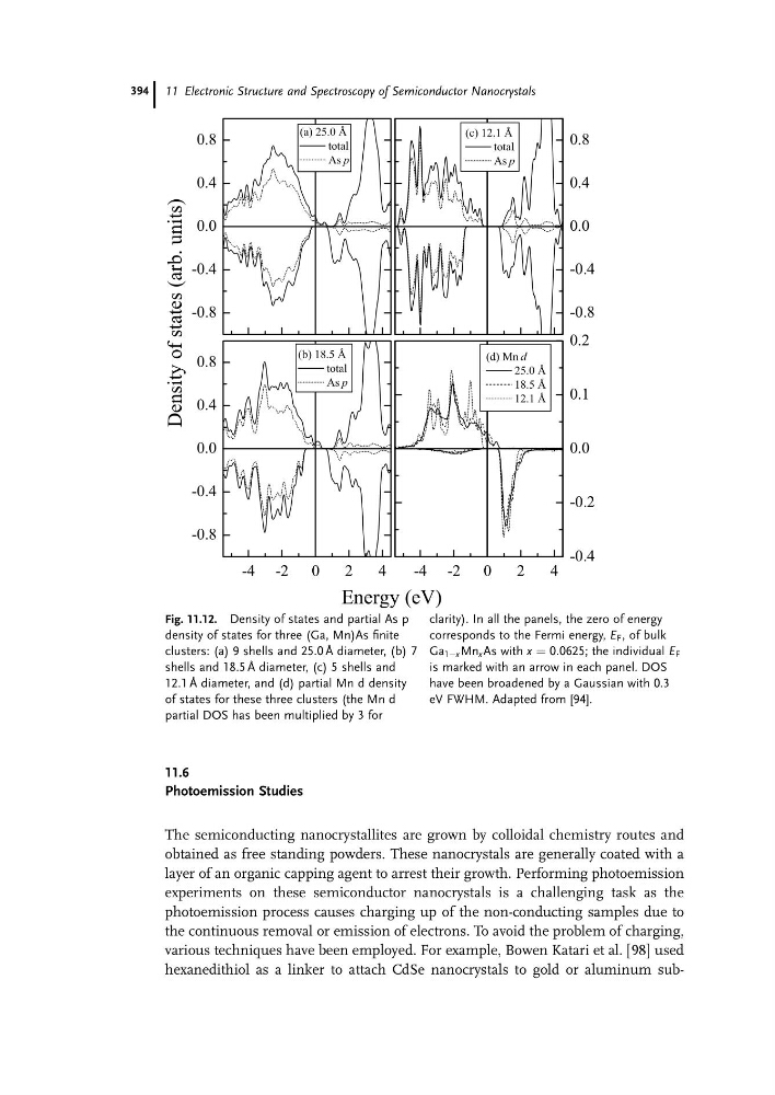
Fig. 11.12. Density of states and partial As p
density of states for three (Ga, Mn)As finite
clusters: (a) 9 shells and 25.0 A ˚ diameter, (b) 7
shells and 18.5 A ˚ diameter, (c) 5 shells and
12.1 A ˚ diameter, and (d) partial Mn d density
of states for these three clusters (the Mn d
partial DOS has been multiplied by 3 for
clarity). In all the panels, the zero of energy
corresponds to the Fermi energy, E F , of bulk
Ga 1Àx Mn x As with x ¼ 0:0625; the individual E F
is marked with an arrow in each panel. DOS
have been broadened by a Gaussian with 0.3
eV FWHM. Adapted from [94].
11 Electronic Structure and Spectroscopy of Semiconductor Nanocrystals
394
Photoemission Studies
The semiconducting nanocrystallites are grown by colloidal chemistry routes and
obtained as free standing powders. These nanocrystals are generally coated with a
layer of an organic capping agent to arrest their growth. Performing photoemission
experiments on these semiconductor nanocrystals is a challenging task as the
photoemission process causes charging up of the non-conducting samples due to
the continuous removal or emission of electrons. To avoid the problem of charging,
various techniques have been employed. For example, Bowen Katari et al. [98] used
hexanedithiol as a linker to attach CdSe nanocrystals to gold or aluminum sub0.0
0.4
0.8
-0.8
-0.4
0.0
0.4
0.8
-4 -2 0
2
4
-0.8
-0.4
0.0
0.4
0.8
-0.8
-0.4
0.0
0.1
0.2
-4 -2 0
2
4
-0.4
-0.2
(c) 12.1 Å
total
As p
(b) 18.5 Å
total
As p
(a) 25.0 Å
total
As p
Density of states (arb. units)
Energy (eV)
(d) Mn d
25.0 Å
18.5 Å
12.1 Å
Fig. 11.12. Density of states and partial As p
density of states for three (Ga, Mn)As finite
clusters: (a) 9 shells and 25.0 A ˚ diameter, (b) 7
shells and 18.5 A ˚ diameter, (c) 5 shells and
12.1 A ˚ diameter, and (d) partial Mn d density
of states for these three clusters (the Mn d
partial DOS has been multiplied by 3 for
clarity). In all the panels, the zero of energy
corresponds to the Fermi energy, E F , of bulk
Ga 1Àx Mn x As with x ¼ 0:0625; the individual E F
is marked with an arrow in each panel. DOS
have been broadened by a Gaussian with 0.3
eV FWHM. Adapted from [94].
11 Electronic Structure and Spectroscopy of Semiconductor Nanocrystals
394